This post documents some of the tips and tricks I learned while integrating ESP8266 into my own circuit designs. Some of them help reduce the components needed thus minimizing the cost, while others have to do with selecting and using GPIO pins. For breadboard prototyping, you can certainly use one of the popular ESP8266 development boards, like NodeMCU, WeMos etc. But what I want to cover in this post is to integrate a ESP8266 module (such as ESP-12F) into the circuit design, without using the development boards.
In the past several years, I’ve gradually transitioned all my gadgets from using the classic ATmega chips (including ATmega328 and ATmega1284) to ESP8266. There are a lot of advantages of ESP8266: it has built-in WiFi, it’s Arduino compatible, it has a lot more RAM and flash memory space than the classic ATmega chips, and it’s really cheap. In fact, due to the ongoing chip shortage, the ATmega chips have become more expensive and difficult to source, while ESP8266 is still widely available at a very cheap price. ESP8266 certainly has some downsides as well: it has a relatively small number of GPIO pins, particularly, it has only one analog pin, which limits its applications; also it can be tricky to use in low-power applications driven by battery power. Nonetheless, as most of my gadgets are powered by USB (+5V), ESP8266 is a perfect choice for me.
Power Circuit
The operating voltage range of ESP8266 is 2.5~3.6V, with 3.3V being the most common. If the input voltage is 5V (from USB), a common method is to use a 3.3V linear voltage regulator, such as AMS1117-3.3. At first, I thought that pretty much any jellybean 3.3V regulator would be sufficient. However, it turns out that ESP8266 can draw a fairly large amount of surge current instantaneously, so some cheap regulators I’ve tried, such as XC6206-3.3V, does not work reliably at all, even though on paper it claims to handle a maximum current of 250mA.
Now, from 5V to 3.3V there is a 1.7V voltage drop, which is about 2 diode drops. Realizing this, I found that a very cheap and quite reliable method to provide power to ESP8266 is to simply use two 1N4148 diodes in series. Under the typical current draw of ESP8266, each diode drops about 0.75~0.85V; with two of them in series, the voltage comes out to be almost exactly 3.3V. Also, as diodes can handle instantaneous current surge quite well, this method works quite reliably, compared to some of the weak voltage regulators.
On the output of the two diodes, you do need a 100~220uF to provide a sufficient buffer. However, since the voltage is low (~3.3V), the capacitor isn’t necessarily large in physical size. A 100uF electrolytic or tantalum capacitor rated at 6.3V or 10V should work just fine. The schematic below shows this simple power circuit.
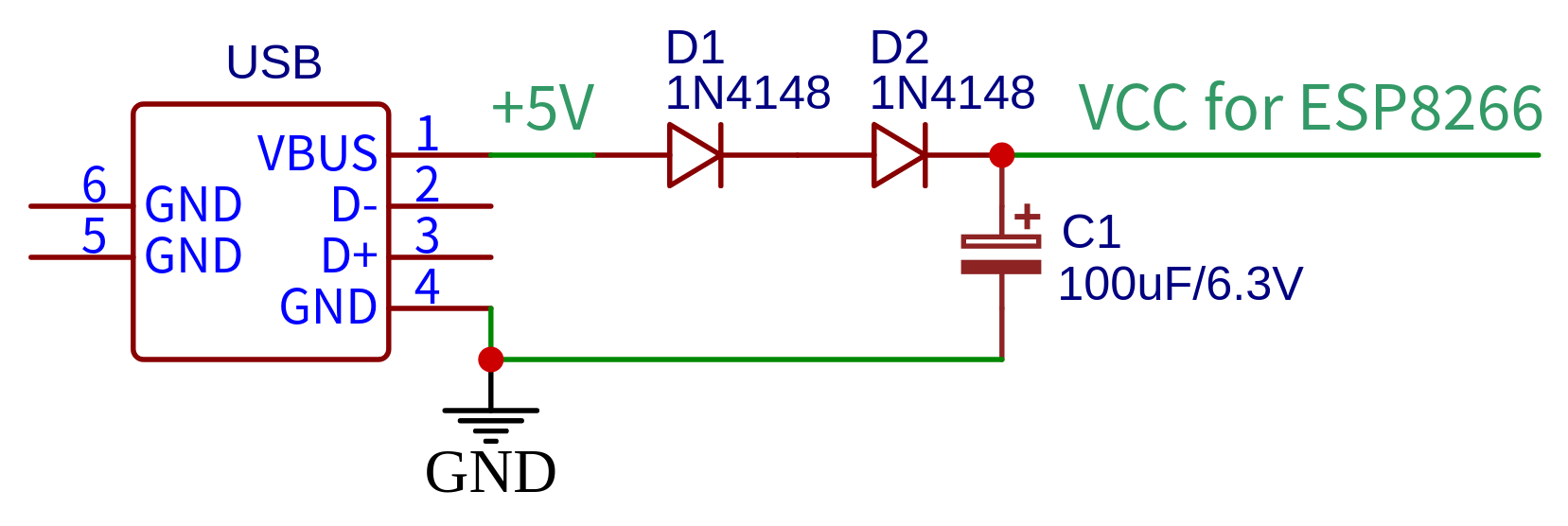
Note the assumption is that the input voltage is from a +5V USB power source, which can provide a minimum of 500mA stable output current. This is indeed the most common case for me. If the input voltage is much higher than 5V, you will still need a voltage regulator. In fact, if the input voltage is significantly higher than 5V, you likely will need a switching regulator for efficiency reasons.
I’ve also had several cases where the gadget need to be powered from USB as well as a lithium battery. The above diode-based power circuit can be easily extended to support dual power sources, as shown below.
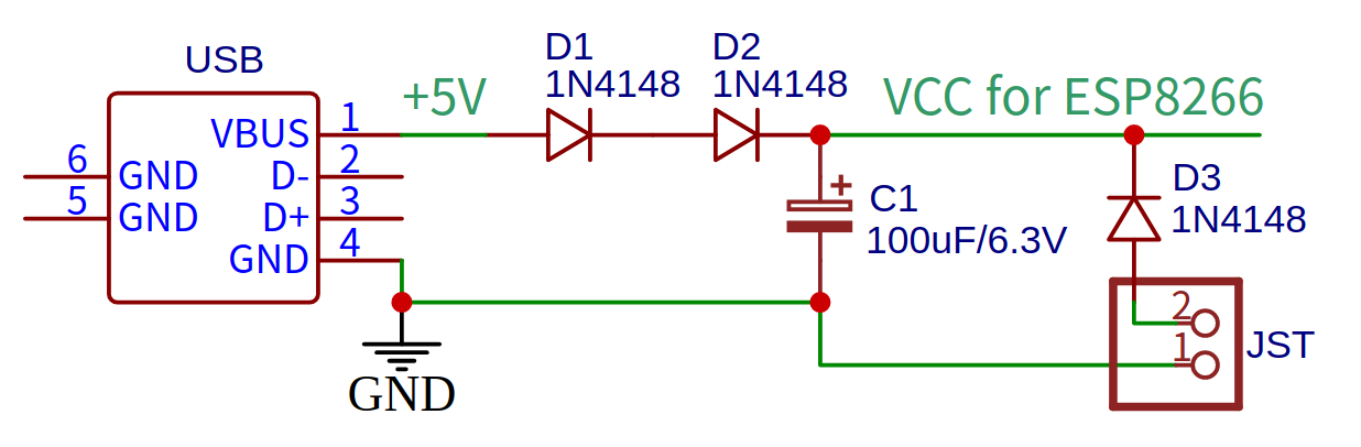
Here JST is a lithium battery connector. Diode D3 provides the necessary voltage drop: a standard single-cell lithium battery gives 3.7~4.2V, so after D3 it becomes 3~3.5V, which is within the operating voltage of ESP8266. D3 also blocks reverse current in case both USB and lithium battery are plugged in at the same time. This way, at any given time, only one of the two sources will be automatically selected to provide current to ESP8266.
This circuit can also be extended to support charging of lithium battery through USB, such as by using the popular TP4054 battery charger. The input of the charger is 5V from USB, and output is pin 2 of the JST connector. This way, the lithium battery can be connected at all times, and it will be charged whenever USB is plugged in.
Auto-Reset Circuit
A very convenient feature of ESP8266 development boards is the auto-reset circuit: when programming ESP8266, the auto-reset circuit triggers the bootloading sequence automatically before sketch uploading starts, thus there is no need to press any button to manually enter the bootloading mode. This is accomplished by toggling pins on the USB-serial chip with appropriate timing sequence, to simulate a reset while GPIO0 is being held low.
Using CH340 (a very popular, low-cost USB-serial chip) as example: the typical auto-reset circuit such as used on NodeMCU, is as follows:
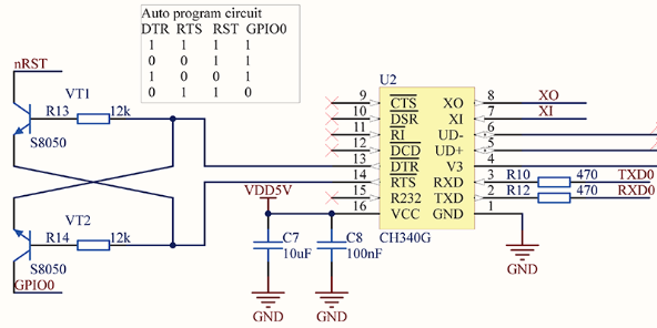
Here the DTR and RTS pins on CH340 are connected to the auto-reset circuit involving two resistors and two NPN transistors. My understanding is that the two transistors are essentially level-shifting circuits, because in the schematic here, CH340 operates at 5V, while ESP8266 operates at 3.3V.
However, CH340 can operate perfectly fine under 3.3V. So if we power CH340 and ESP8266 both with 3.3V, then there is no need to use the level shifting circuits, saving two resistors and two transistors. Below is my simplified auto-reset circuit:
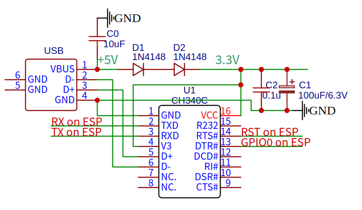
Note that this circuit uses the CH340C variant of the CH340 chip (there are several variants: G, C, B, T, etc.) because it has built-in 12MHz oscillator, thus there is no need to connect an external crystal oscillator. Also, note that the V3 pin is connected to 3.3V, this is required if it’s CH340 is powered by 3.3V. The TXD, RXD, RTS, and DTR pins on CH340 are connected to RX, TX, RST (Reset) and GPIO0 pins on ESP8266 respectively. No more NPN transistors for level shifting.
GPIO10 comes handy when you really need one more GPIO
If you are familiar with ESP8266, you are probably aware of the typical set of available GPIO pins. These are:
- GPIO0: the bootloading indicator pin, usually pulled high, can be used as a button if needed.
- GPIO1/3: the default TX/RX pins, generally connected to the USB-serial chip as above.
- GPIO2: connected to the built-in LED on ESP12-F, active low. Must be pulled high at booting.
- GPIO4/5: the default I2C pins. I generally use them for connecting to I2C components like SSD1306 OLED display, real-time clock etc.
- GPIO12/13/14: general-purpose IO pins that are good for anything; support interrupts and internal pull-ups. These are also the hardware SPI’s MISO, MOSI, and SCK pins, so you will need them if you have SPI components like Ethernet modules, external SD card etc.
- GPIO15: must be pulled low at booting. Because this pin is guaranteed to be low at booting, it’s suitable for connecting to output components like a relay, a buzzer, an LED etc. which should be inactive at booting. This is also the hardware SPI’s CS pin, but you don’t have to use it as CS — you can use any GPIO pins as CS pin for SPI.
- GPIO16: this is a restricted pin that does not support interrupt, and has internal pull-down resistor instead of pull-up as the other GPIOs. Other that these restrictions, it can be used as either input or output, but it does have glitches at booting, as detailed below.
As you can see, the number of GPIO pins is quite limited, and those that are truly flexible (i.e. no restrictions and no HIGH/LOW requirements at booting) is even more scarce. What if you just need one more pin? After searching around, I discovered that GPIO10 is another all-around good GPIO pin that you can use. This pin is often not discussed because it’s connected to the internal SPI flash and thus can be problematic to use as GPIO. However, it turns out that this pin is totally usable as long as you make sure the flash mode of ESP8266 is dio (i..e NO qio or qout mode: they will cause GPIO10 to be unusable). Other than that, you can use GPIO10 as input or output, it supports interrupt and internal pull-up.
Some of the forums also mention GPIO9: unfortunately this doesn’t seem to be usable at all. I’ve tried and it always gets my ESP8266 stuck so I gave up.
If you need a lot more GPIO pins, check out my previous post about IO expander chips — it talks about different IO expander options and their pros and cons.
Using a GPIO pin to indicate hardware revision
Occasionally I make changes to a circuit, which often involves re-assigning GPIO pins for different components. For example, in the initial version of a circuit, I assigned GPIO15 to a buzzer; then in a later revision, I ended up removing the buzzer and re-assigning GPIO15 to the CS pin of an Ethernet module. With these different hardware revisions, it’s necessary to also make firmware changes. But I don’t want to maintain so many different versions of the code. Instead, I want the same firmware to automatically detect which hardware revision it is. A common trick I’ve used is to dedicate a spare GPIO pin for this purpose. The way this works is that all GPIO pins on ESP8266 have internal pull-ups (except GPIO16, which has an internal pull-down and not up). The resistance on these pull-ups (or down) is about 40 to 60 Kohm. So assuming nothing is connected to a pin, if you turn on the internal pull-up, it should read HIGH right after booting up. To indicate a different hardware revision, you can connect the pin with a resistor to ground (the resistor value can be anywhere between 1~10 K). This way, the pin will read a LOW even as internal pull-up is enabled. This can be used as an indicator for a different hardware revision.
Of course the downside of this method is that it sacrifices a GPIO pin. But some pins, like GPIO16, has some restrictions that make them less useful than other pins, so why not dedicate it as a revision indicator 🙂
Getting Rid of CH340
So in the above I’ve just talked about how to simplify the auto-reset circuit to save two resistors and NPN transistors. Now, if I am planning to stay with OTA (over-the-air) firmware update, that is, update firmware through WiFi only and not through USB, then I can even get rid of the CH340 USB-serial chip, saving one entire chip from the circuit design! But wait a minute, I still have to program the initial firmware, so I still need a way to use an external USB-serial adapter to do so!
This can be done by one of several common approaches: for example, you can solder a pin header to the circuit to allow plugging in an external USB-serial adapter; if you don’t even want pin headers, you can get rid of them by using a programmer with pogo pins that, when pressed down, can make temporary contact with the circuit. Along that line, I’ve also made dedicated 3D-printed programming assemblies like in the pictures shown below:
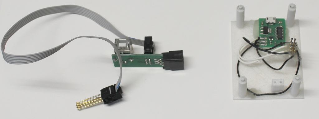
After experimenting with various methods, my favorite one at the moment is to use a card-edge connector that can directly plug into the circuit board. This is basically like the pin-header approach but without having to solder anything. Specifically, I made a custom programmer with CH340 and a 2×3 card edge connector. Then on the circuit board containing ESP8266, I make a matching section, using cutouts and SMD pads, to plug into the connector of the programmer. Standard PCB thickness is 1.6mm, which is perfect for the card edge connector. This idea is very similar to those circuits you may have seen that directly plug into a USB port, or those business-card USB gadgets.
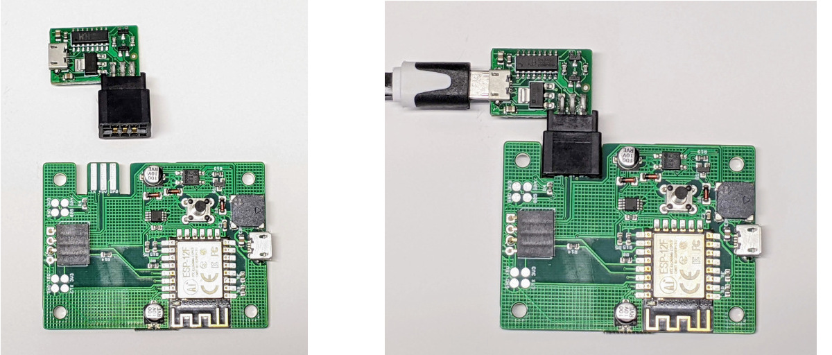
What, you may ask, motivates this level of cost-cutting? Well, the ongoing chip shortage has made many parts more expensive and/or difficult to source, so saving a part is not only saving the cost, but also reducing the likelihood that I can’t finish the project because I am short of a 50-cent part. To me, the card edge connector is quite reliable, and there is no problem with pin alignment or accidentally bent pins which I encountered when using the pogo pins.
Choosing the right GPIO pins for the components
Not only ESP8266 has a small number of GPIO pins, but some of them have ‘quirks’ or ‘glitches’ at power-up that you must be aware of when choosing pins for various peripheral components. There are several online articles that discuss ESP8266’s pin statuses at booting, such as:
- https://randomnerdtutorials.com/esp8266-pinout-reference-gpios/
- https://rabbithole.wwwdotorg.org/2017/03/28/esp8266-gpio.html
As an example, GPIO16 has ‘glitches’ during booting which make it turn briefly HIGH (i.e. it outputs HIGH instead of is being pulled up HIGH, so no pull-down resistor can keep it LOW during booting). If this is connected to a relay, it can briefly turn the relay on, which may be undesirable. As another example, GPIO15 must be kept low during booting (otherwise booting fails), but if you use it as CS (chip select) of an SPI component, pulling it low also activates the CS pin, which can cause some random data to be sent to the SPI component. Most likely this is harmless, but if the SPI device is, say, a shift register, this may end up setting the shift register briefly in random states until the setup code kicks in to clear out the shift register values.
As a concluding remark: ESP8266 has served me really well in the past several years. Although the lack of GPIO pins and the ‘quirks’ on various pins are major drawbacks, sometimes I feel these restrictions turn the circuit design into a ‘constraint satisfaction’ problem, which can be an interesting puzzle to solve than a total annoyance. On the other hand, ESP8266’s bigger sister ESP32 has become a lot more popular as well: it has abundant GPIO pins, many of which have ADC support too, and it has many variants to choose from, some with both built-in WiFi and Bluetooth. I will probably gradually transition to use ESP32 in the future. Some of the methods discussed in this post are likely applicable to ESP32 as well.
