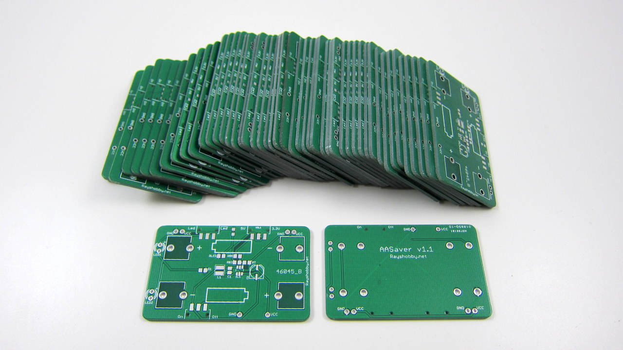
A few weeks ago I received a new batch of the AASaver PCBs at home. I thought, now that I am fairly experienced, it would be interesting to document the process of how I assembled the circuit boards. As you will see below, my assembly setup is manual and is nowhere near the capability of making more than a hundred boards at a time (for that I would outsource the assembly to a professional company). Still, it’s reasonably efficient such that I can enjoy the process of making without losing my mind or temper :).
Step 1. Stenciling
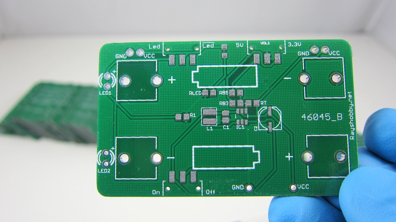
AASaver is designed with all surface mount components. So the first step is to apply solder paste by using a stencil. I used my recently purchased laser cutter to make a stencil out of a Kapton film sheet ordered from Amazon. There are plenty of online tutorials on how to use a laser cutter to make solder paste stencils, so I won’t repeat them here. If you don’t own a laser cutter, you can easily make a stencil using copper sheet with the standard toner transfer and etching method. The tutorial can be found in my previous blog post here. Before I had the laser cutter, I have always used home-made copper stencils, and they work just as good.

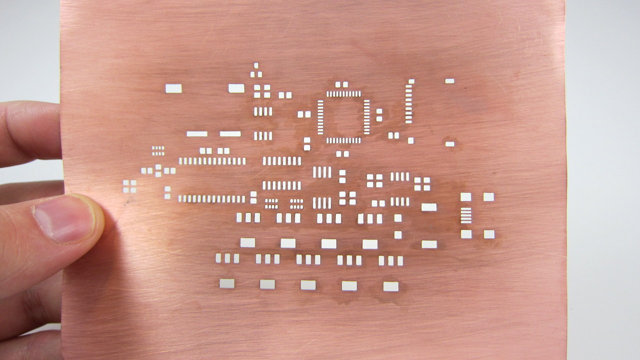
(Left: stencil made from Kapton sheet; Right: stencil made from copper sheet with home PCB method).
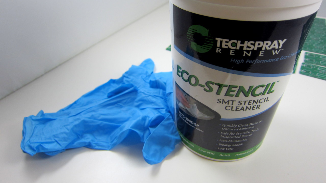
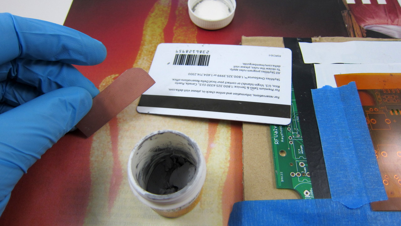
Next, I used old PCBs to make a 3-sided frame that fits the PCB tightly. Then align the stencil with the PCB such that the holes and solder pads match together. I then taped the stencil to the frame for easy lifting up. This allows me to quickly insert and remove a PCB. Since the AASaver board uses fairly big components (0805 and SOT23-6), the alignment does not have to be extremely accurate. Now, before proceeding, you need some tools, including some gloves for hand protection and stencil wipes for cleaning (both are available from from Amazon),
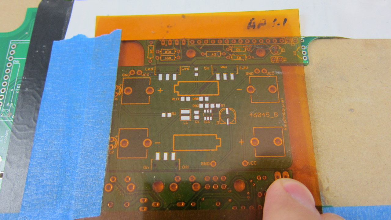
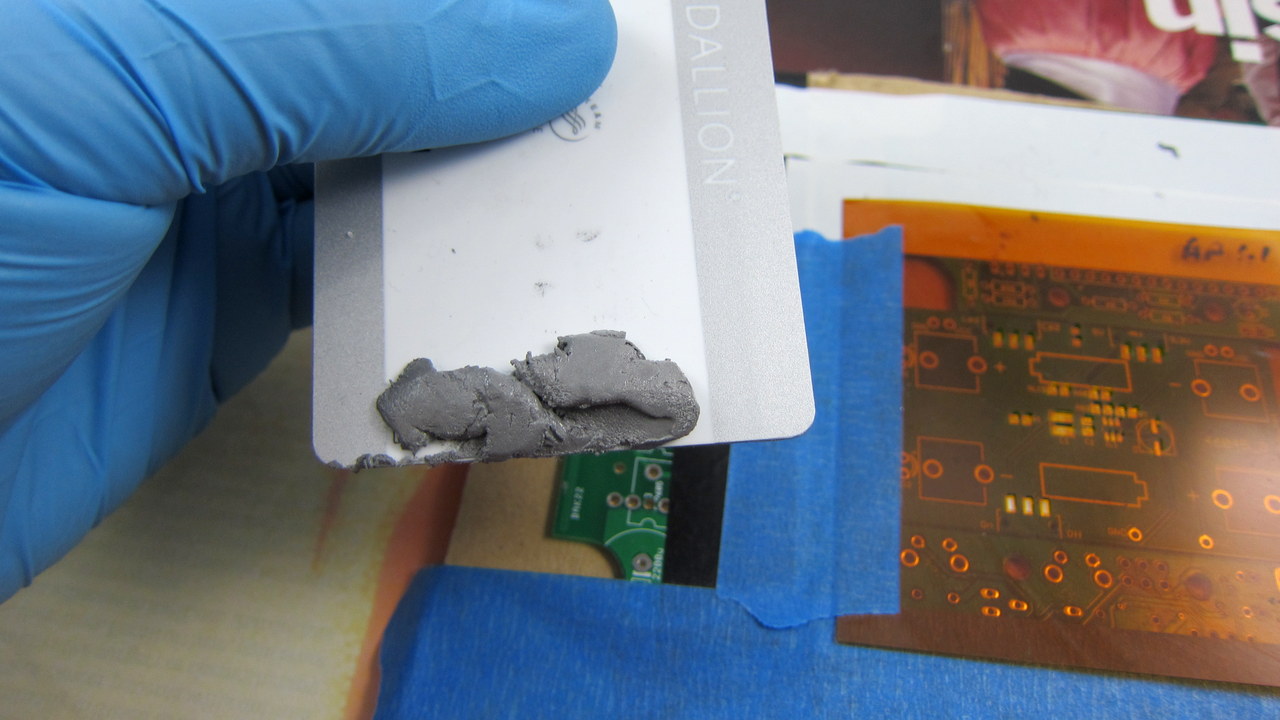
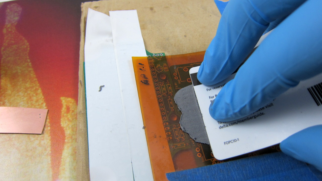
as well as solder paste (which I got from dealextreme.com) and a credit or membership card as applicator. Now, put a sizable amount of solder paste onto the applicator, and then start pressing it down onto the stencil. I usually do two passes: the first swipe leaves a thick layer of solder paste; then the immediate second pass scrapes the excessive paste off the stencil sheet. Use only medium pressure — you don’t need to press very hard. After stenciling, lift up the stencil and remove the PCB from the frame. Check the solder paste on each pad and make sure everything looks ok. If something is wrong, use stencil wipe to clean the solder paste off the PCB and start over.
The stenciling step doesn’t take much time. Once you are experienced, you can do it quite quickly: finishing 100 AASaver PCBs took me less than 20 minutes.
Step 2. Populating Components
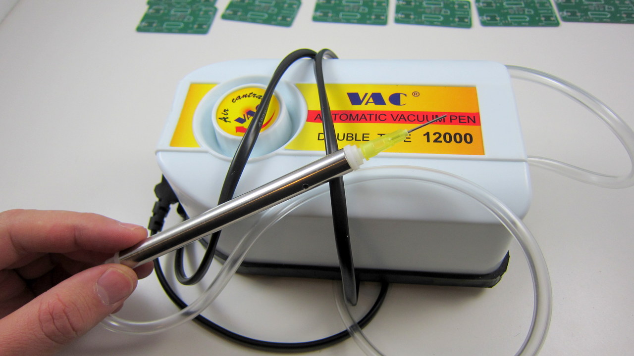
The second step is populating components onto the PCB. This is the most time consuming step and you will probably want to take short breaks in between :). I used to do it with tweezers, which required a lot of patience. Recently I discovered a couple of tools that can help increase productivity quite a bit. The first tool is a vacuum pen. It comes with a portable vacuum pump, two plastic tubes, and a pen with several different needle sizes. This is available on eBay if you search ‘pick and place vacuum pen‘. Be careful that the unit only works with 220V (designed for Chinese market). So in order to use it with 110V, you need a step-up transformer, which I got from Amazon for about 7 bucks. Well, if you plug it directly into 110V power line, there shouldn’t be any damage, the pump probably just won’t start.

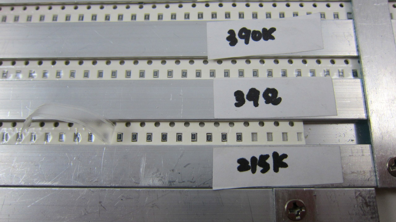
The second tool I discovered is the SMT feeder. Again, this is available from eBay by searching ‘SMT feeder‘. These are similar to feeders found on automatic pick and place machines, except they are static and do not automatically advance the tapes. I made some labels to help me remember the components on each line.
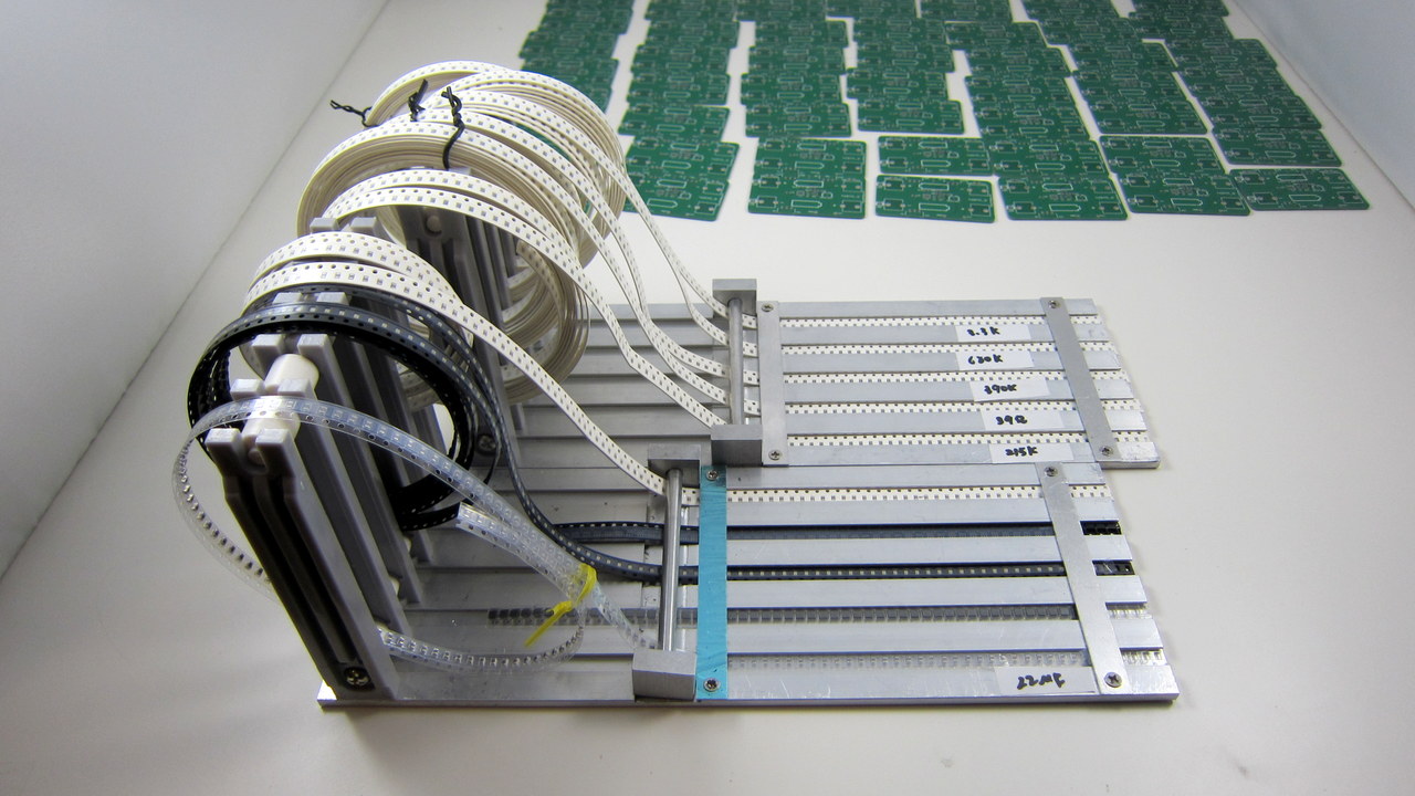
With these tools, placing components is much easier than using tweezers: I no longer have to dump components out of the tape, or flip components to face up, or spend a lot of time adjusting the orientation of the components. Such a time saver :).
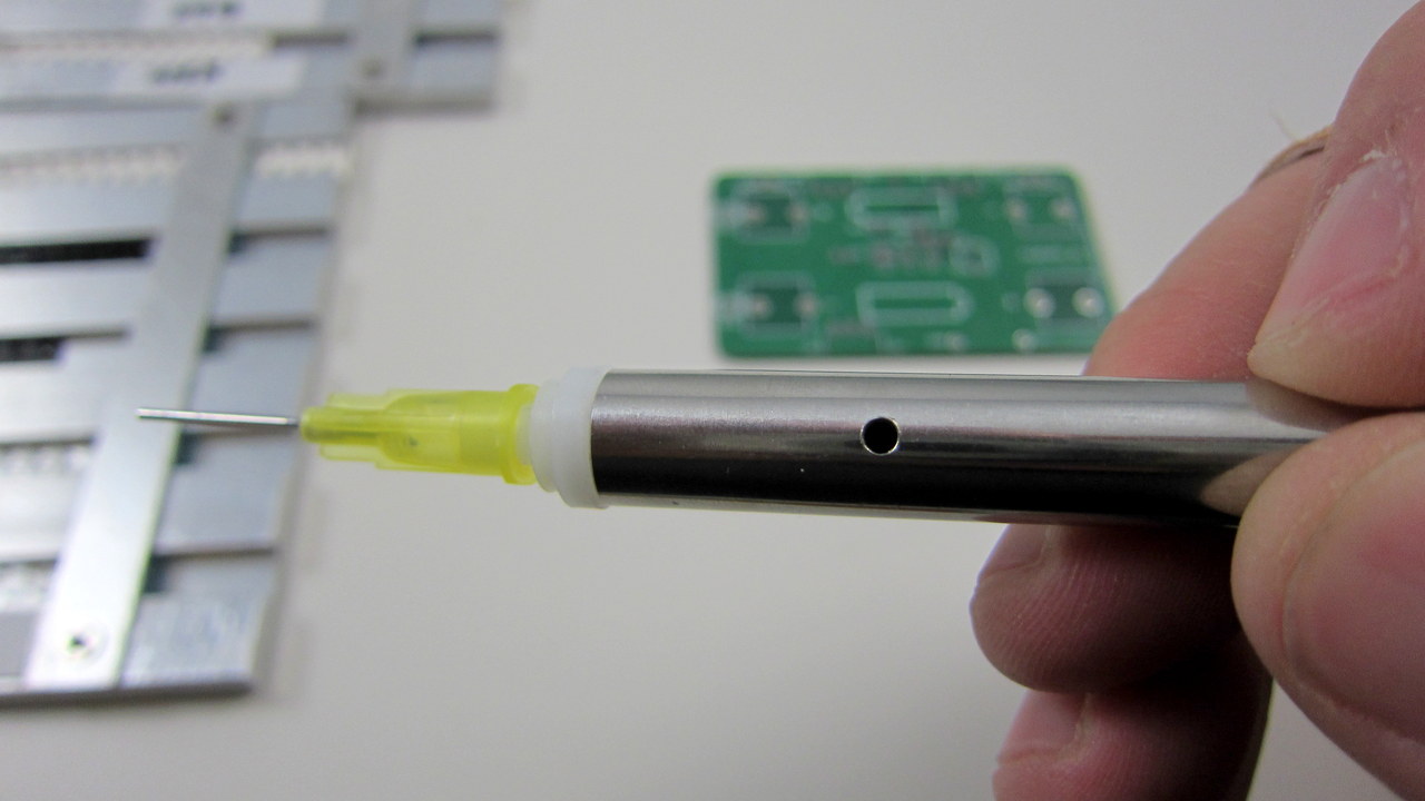
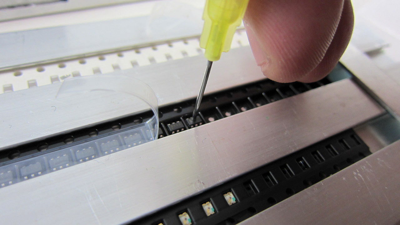
So how do you use the vacuum pen? Notice that on the side of the pen there is a small hole. When you cover the hole with a finger, it creates vacuum suction pressure through the needle of the pen, which allows picking up components. Then when you remove your finger, the air flows through the hole, and releases the component from the needle. I typically use my index finger for this.
To demonstrate: first, get the needle close to a component and cover the hole; then pick up the component (as long as your finger covers the hole, the component won’t fall off); finally, carefully approach the PCB, press down the component to where it should be placed, and release the finger. The placing step definitely requires some practice. You can use your other hand to help stabilize the movement and the ‘touch-down’.
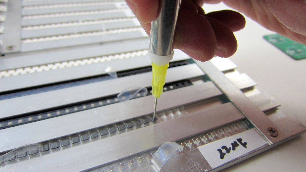
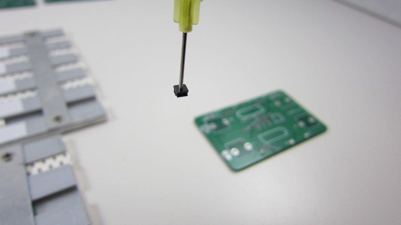
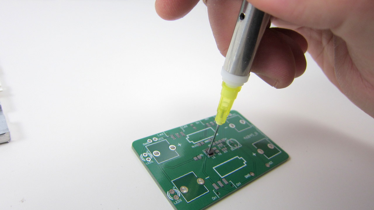
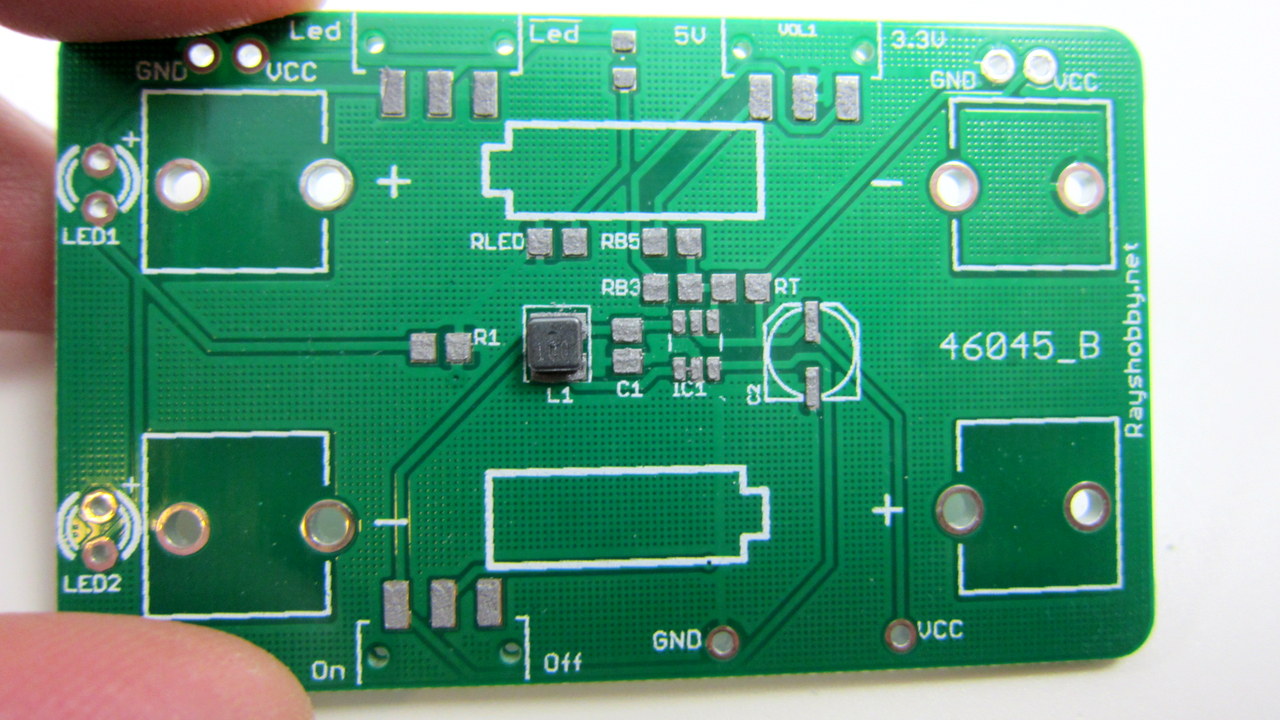
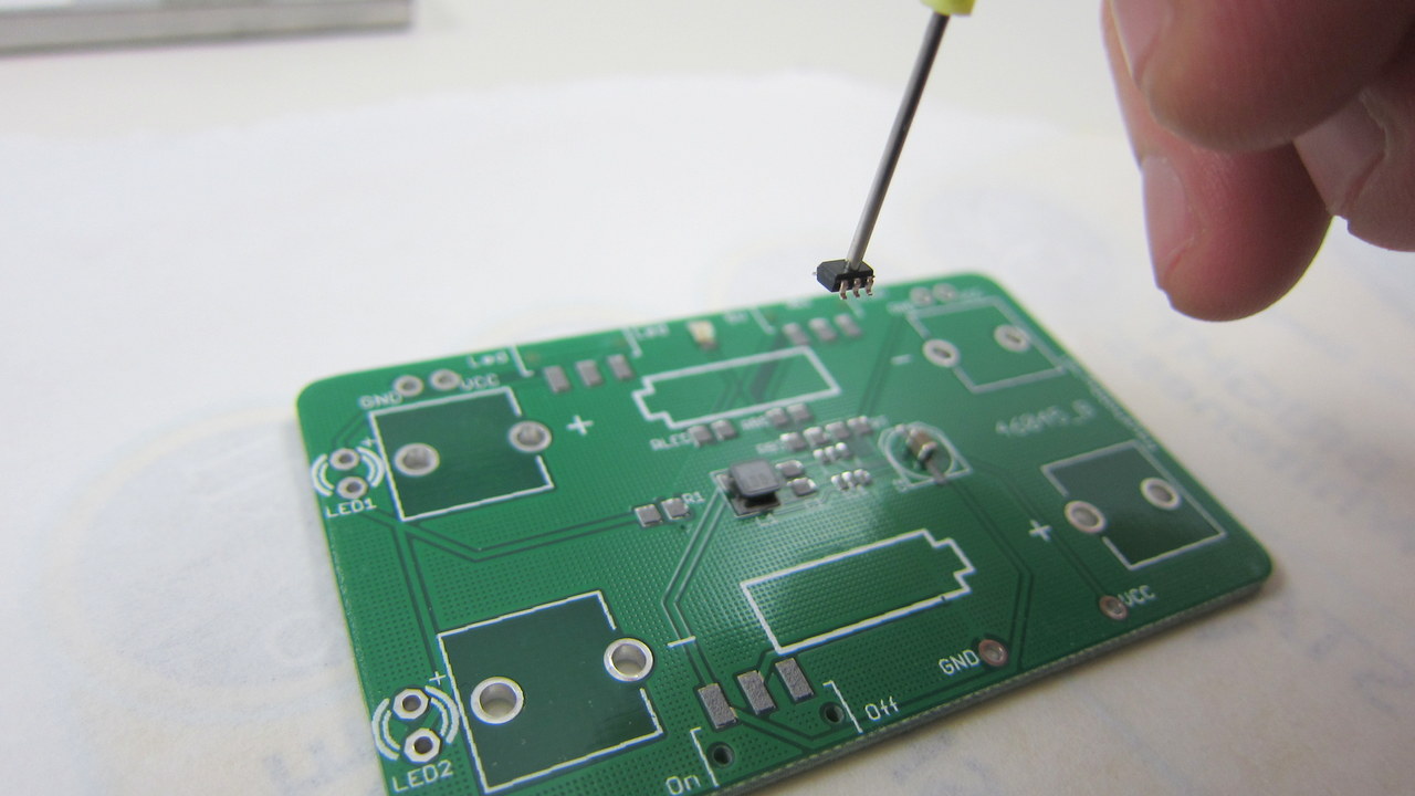
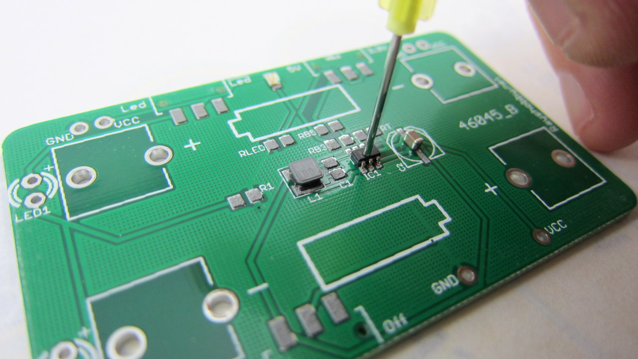
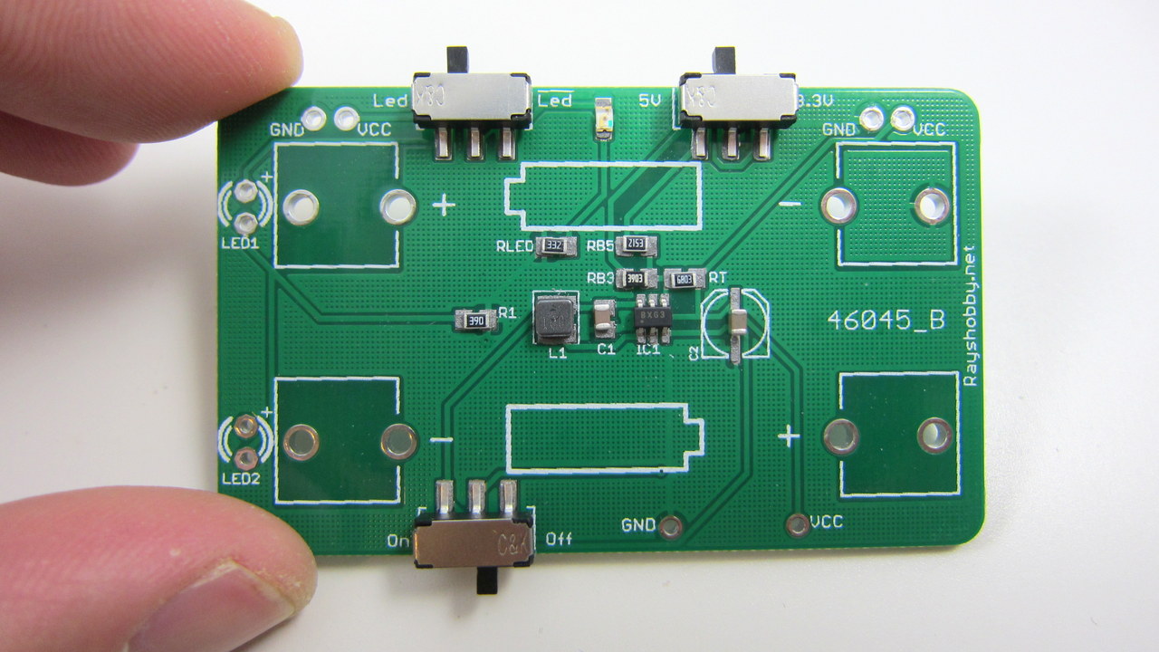
The first few times I used the pen, I was shocked at how poorly the components were placed. I felt it’s a complete piece of junk. But then as I used it more, I realized that I do get more experienced with practising (feels kind of like playing a video game :). Anyways, now I can place components at pretty good speed and accuracy. Practice maker perfect. Note that sometimes you need to change the orientation of a component, and that can be done by simply rotating the PCB around with your other hand. Here is another example of picking and placing an SOT23-6 component, and lastly a picture of the fully-populated board:
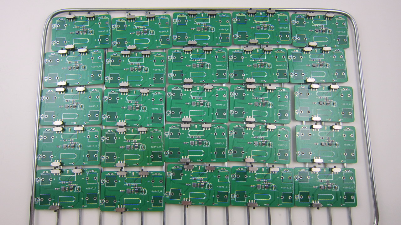
These are 25 boards that have components placed and ready to be toasted:

Step 3. Reflow Soldering
The next step is the fun step, which is the ‘cook’ the PCBs so that the components will be reflow soldered onto the boards. I used to do this step with a toaster oven and a digital thermometer to monitor the temperature. Because I was lazy, I didn’t implement any sort of feedback control. As a result, there were a couple of times that I ‘over-cooked’ the PCBs till they burned and smelled terribly. So I decided to buy a real reflow oven. The one I purchased is model T-962A from eBay (which used to sell at ~$400 but is now more expensive). Note that its sister model T-962 is cheaper but also has a much smaller soldering area.
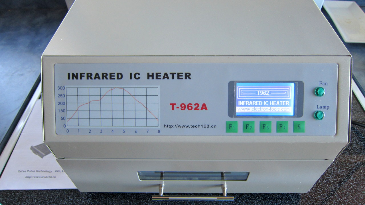
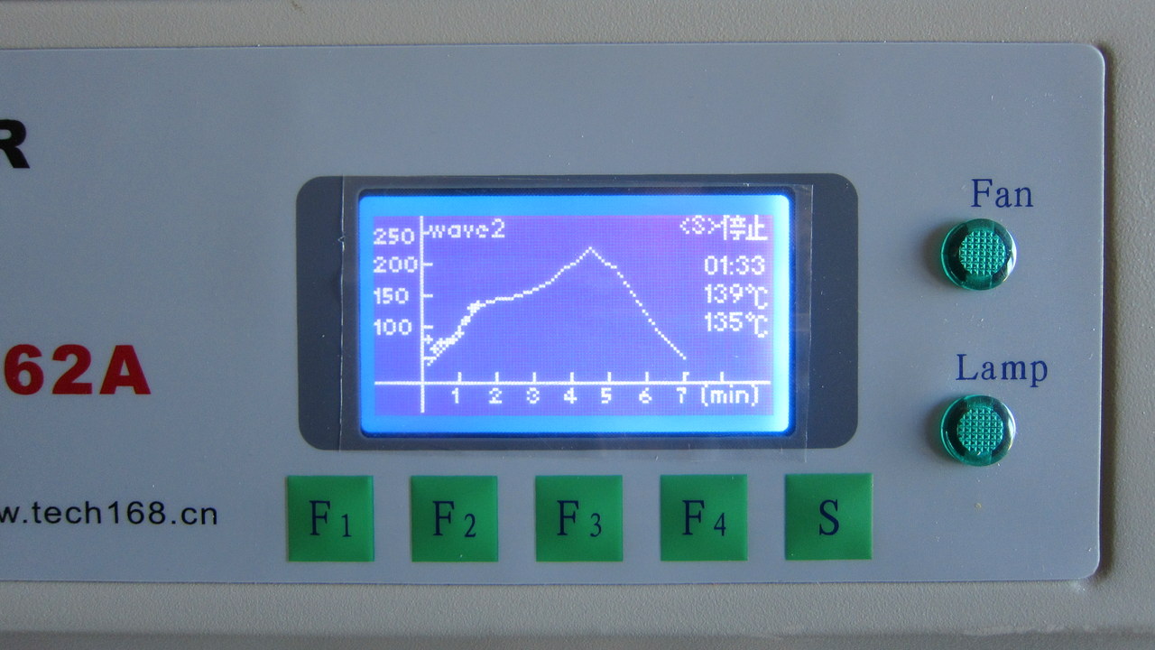
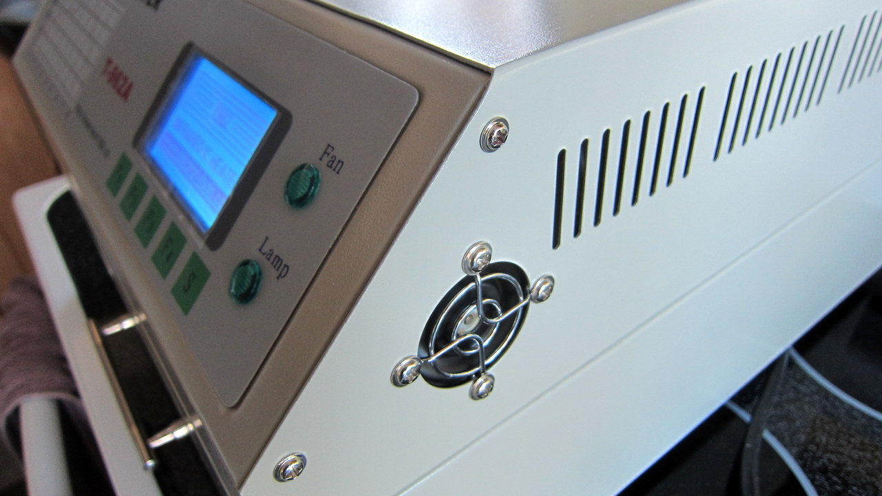
This reflow oven does the basic stuff: it lets you select a pre-programmed reflow temperature profile, or program a custom profile if you want; it follows the selected profile quite accurately, by using an internal infared heating element, a cooling fan, and microcontroller-based feedback control; it also has a glass slit window on the front to allow you to monitor what’s happening inside the drawer. The user manual even describes how to use it to solder double-sided PCBs, which I haven’t tried yet.
The oven also has its drawbacks: the standard profile takes 7~8 minutes to finish one cycle of reflowing, which is not very fast but perhaps can be accelerated using a custom profile; also, the heating is not entirely uniform — the area close to the boundary is cooler than the center, causing PCBs placed nearby the boundary to be poorly soldered. But once I am aware of these limitations, I can cope with them.
One important thing to keep in mind is that you should place the reflow oven outdoors. Even with lead-free solder paste, the exhaust from the reflow process is unpleasant at least, and probably harmful to your health. So keep it out of your living area.
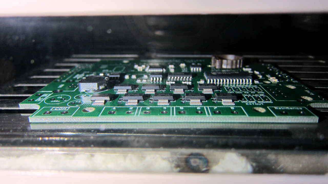
Once the reflow is done, I get back a tray of freshly baked ‘cookies’. Satisfied 🙂 Take a close look at the PCBs and see if everything looks ok. Especially check if there are any un-soldered paste. If so, put them back and bake again.

Step 4. Testing
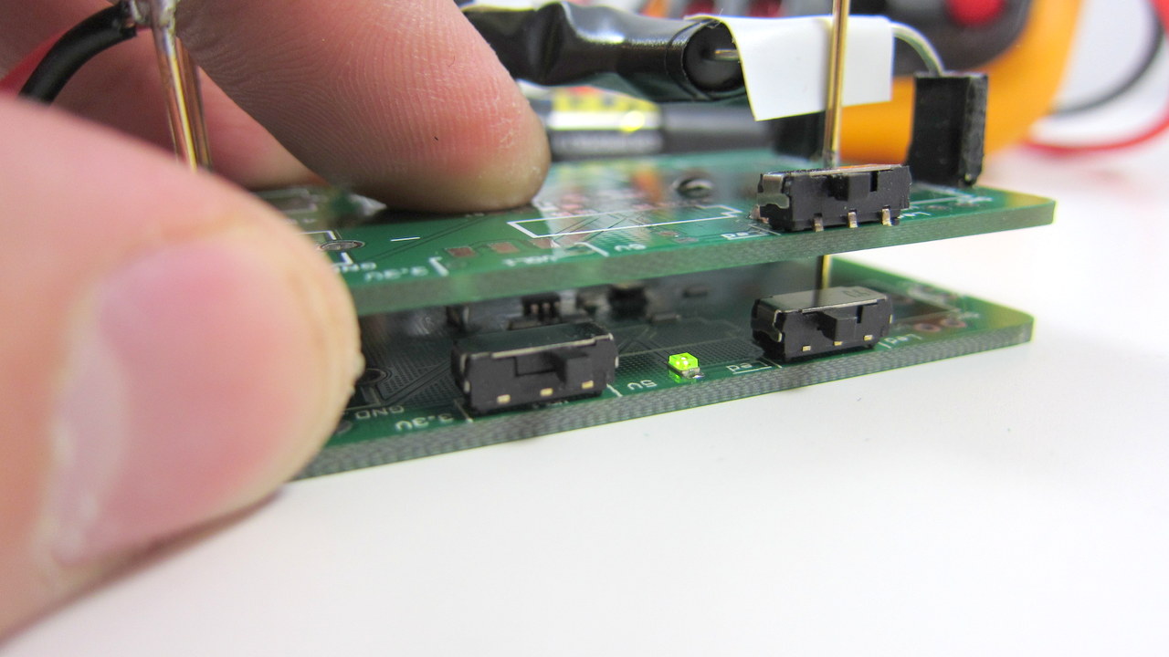
We are not done yet, so don’t bite. The last step is testing, to make sure the circuit board functions as expected. First, perform a quick visual examination. Occasionally components may drift off its position, probably due to insufficient solder paste. These are easy to fix with a hot air gun or even a standard soldering iron. To facilitate testing, I built a simple rig using an existing AASaver PCB and some pogo pins I got from eBay. Here is my setup:
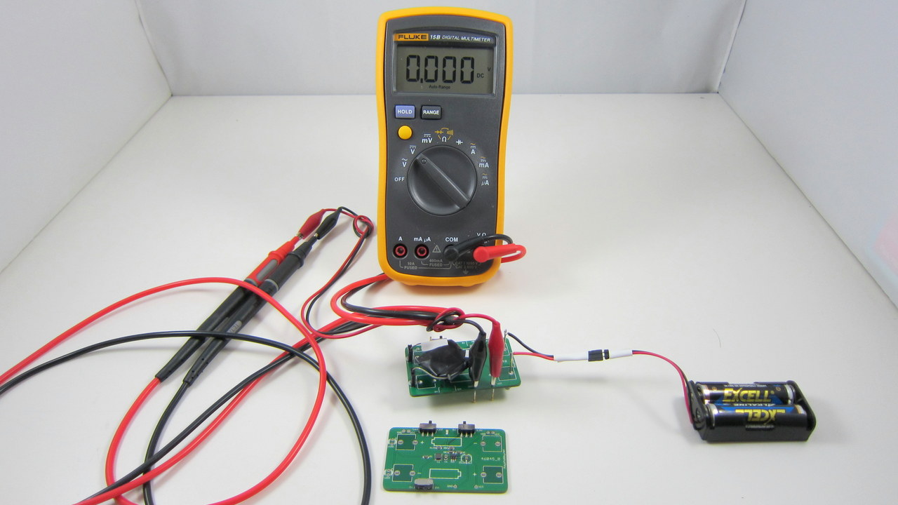
Because AASaver is a regulated voltage booster, the main things I need to test are whether its output voltages are within spec (5V and 3.3V), and whether it maintains the voltage levels (within 5-10% tolerance) under a given current load (320mA). So my test setup includes a multimeter, AA battery holder, and a power resistor to produce the required current load. If the board passes the test (i.e. outputs and maintains the designed voltage levels with load), it will be put into the ‘success’ bin; otherwise, it will be put into the ‘to-be-fixed’ bin for further checking. For a simple board like AASaver, the success rate (yield) is close to 100%.

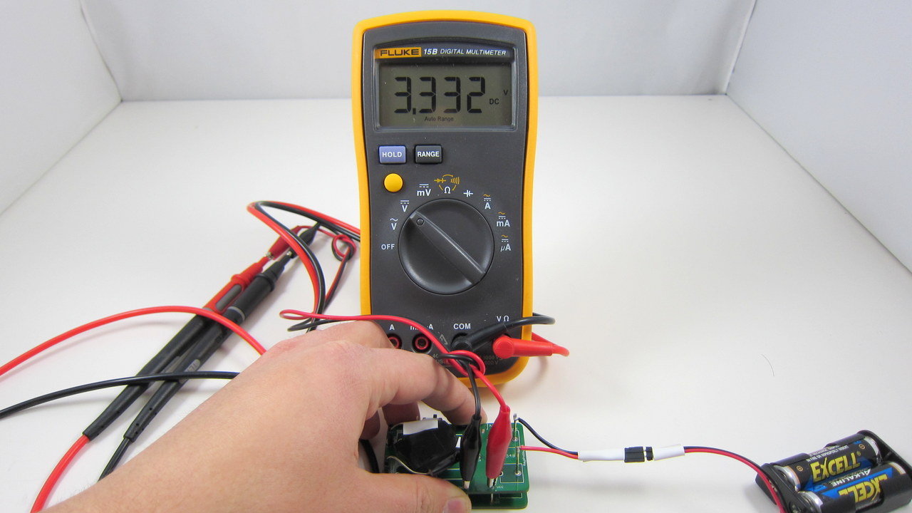
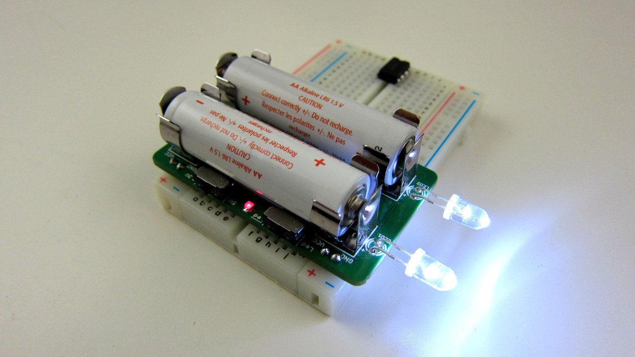
This is a picture of a fully-assembled AASaver in action. It takes two AA batteries, new or used, and can function as an LED flashlight as well as breadboard power supply with switch-selectable 5V and 3.3V output.
That’s all. Feel free to leave your comments, questions, and suggestions. Thanks!
