As I am getting more experienced with the TM-240A pick and place machine (in the following I will call it the PNP machine, as in PNP transistors 🙂 ), I’ve been thinking of ways to improve productivity. One obvious way is to panelize PCBs, meaning to assemble multiple copies of the PCB onto the same board. This can help greatly reduce the overhead time of stenciling and PNP loading time. I have to admit, I’ve never done PCB panelization before. I did search online and found various tutorials, but it’s unclear to me how to exactly indicate the ‘V-cut’ layer to the PCB manufacturer.
But I found an easier route. Recently I’ve been ordering PCBs directly from a Chinese company called ????? (http://www.sz-jlc.com). I got to know this company very randomly, actually through watching the beginning clip of the SparkCore Kickstarter video. The company has a very streamlined PCB manufacturing process, where you can track each step of the PCB making, all the way from drilling, to printing layers, to etching, to optical inspection, to solder-mask and silkscreen printing, to testing, and to shipping. It’s completely amazing (except the website only has Chinese version…). Anyways, when you order PCBs from their website, apparently you can specify how you’d like to panelize your PCBs. You don’t need to panelize the PCB yourself in Eagle (which I haven’t learned how to do yet), but you just need to describe your panel design (like 2×3, 4×4 etc.), and they will do the panelization free of charge. Isn’t that awesome?
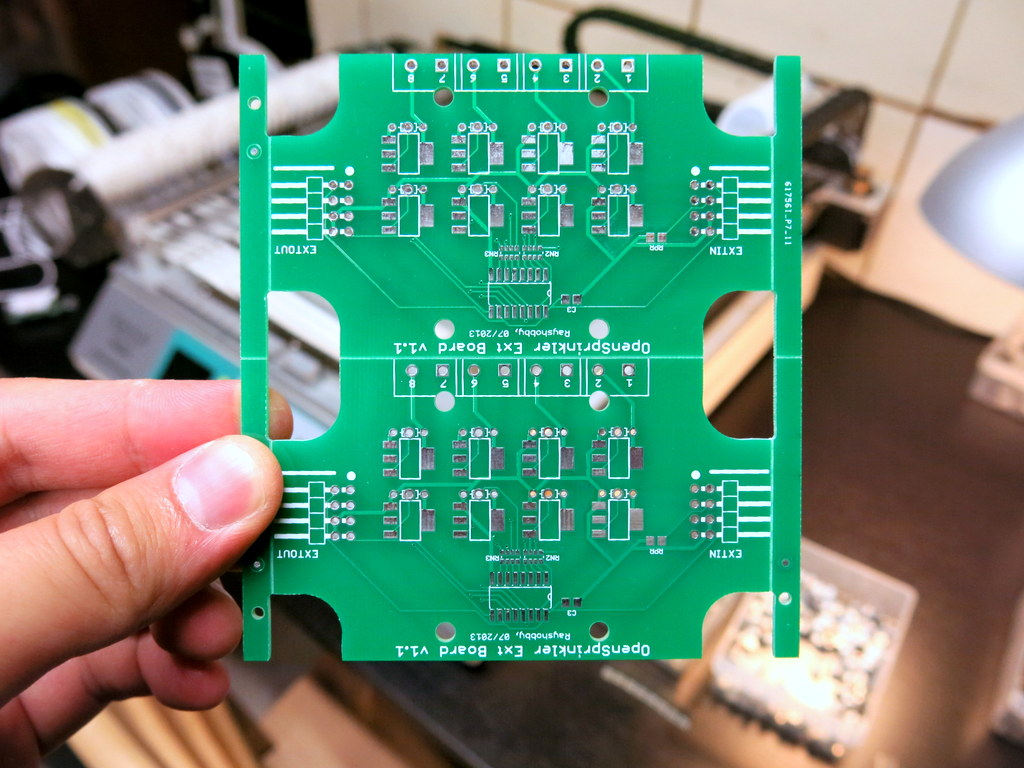
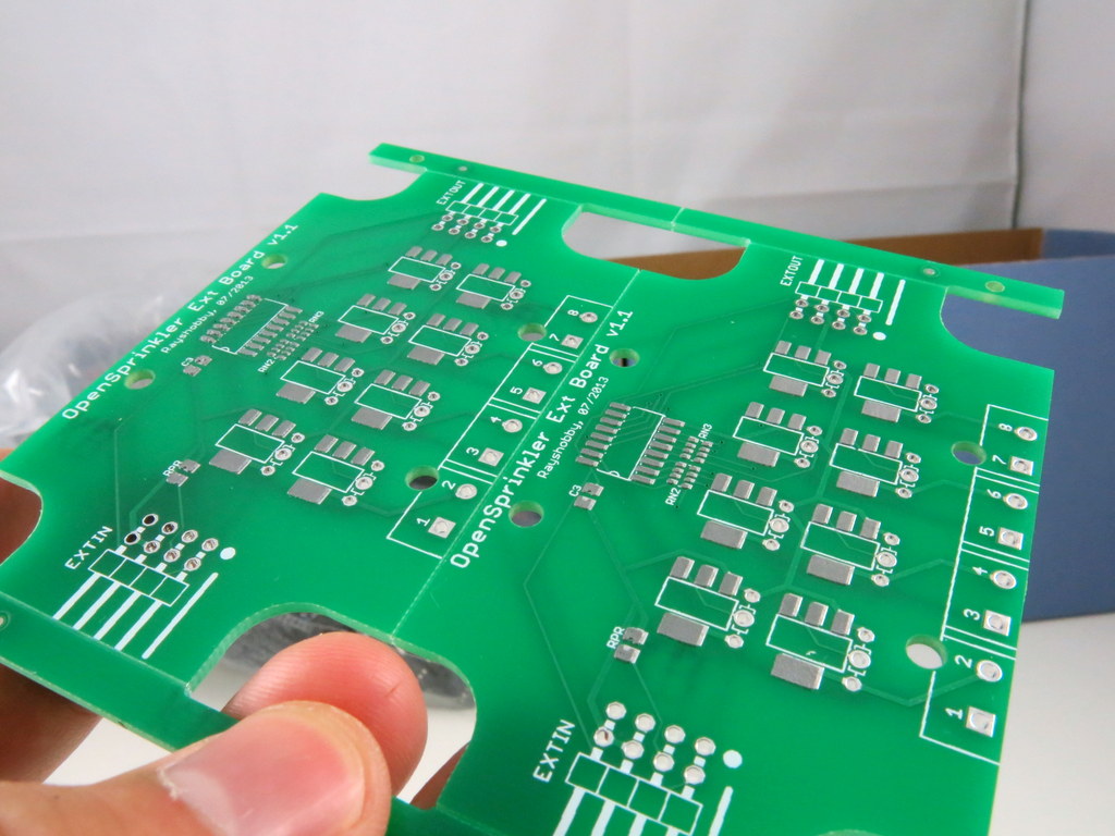
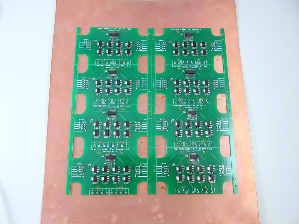
Since this is the first time I’m ordering panelized PCBs, I wanted to be careful. So I ordered a very simple board — the OpenSprinkler Zone Expansion board, with the simplest panelization — 1×2. And the image on the left below shows what I received. Very neat. I also asked them to add an extra 10mm border on each side, and fiducial points (these I paid extra for). Since the board is not rectangular shaped, the panel comes with routed edges on the curved sections, and V-cuts on the straight lines. This way, it can be easily de-panelized by simply snapping each board off along the straight edges. Pretty awesome, especially considering I didn’t have to do anything in Eagle to create the panel design 🙂
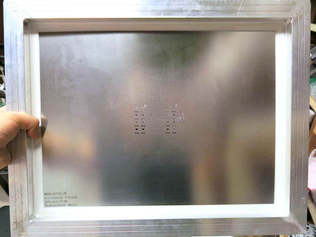
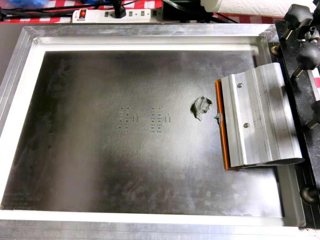
So what’s the picture on the right above? This is also something new to me: apparently when you order PCBs from the company, you can also order a laser-cut solder paste stencil to go with your PCB order. It’s only 10 extra bucks, almost a no-brainer. I ordered one for this particular batch, so I can experiment with it. The stencil is made from a steel sheet, and mounted on a metal frame. It’s quite large (37cm x 47cm), so you will need a stencil printing machine that can handle a board of this size. Fortunately I got a fairly big manual stencil printing machine a while back, so I can put it to good use now.
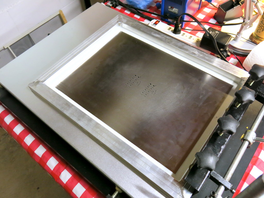
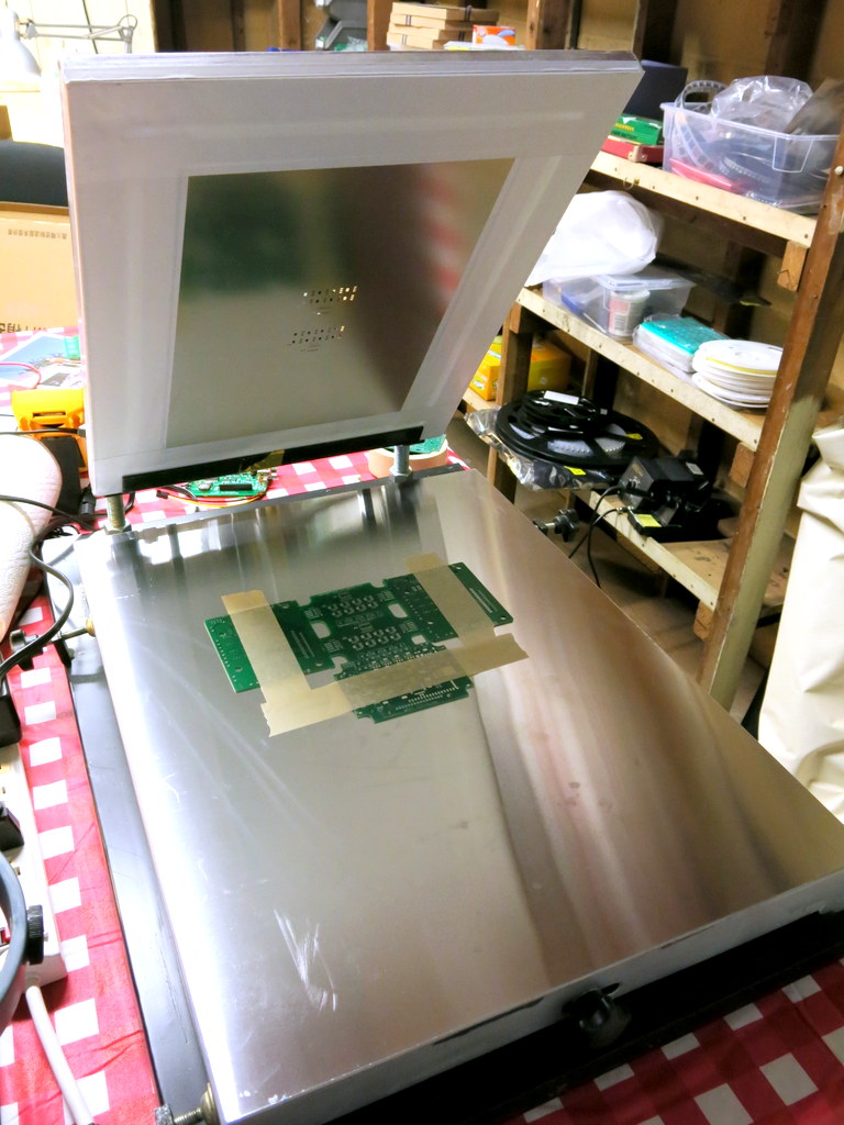
In order to use the stencil, the first thing I did was to mount the stencil frame onto the printing machine. Once mounted, you can easily lift the stencil up and down, to quickly insert and take out stenciled PCBs. Then I aligned the PCB to the stencil holes. This is very tedious — since the stencil is made of steel, which is opaque, there is no easy way to align them. I had to do a lot of trial and error and eventually was able to get them perfectly aligned. Once aligned, temporarily fix the PCB in place by using some tape. Finally, use three old PCBs to make a frame around the center PCB. Then you are all set.
With the stencil printing machine (albeit manual), applying solder paste works like a charm, and is much faster than using my home-made stencils. The stenciling quality is also excellent (see the picture on the right below). Apparently they optimized the stencil design, and created small ‘crosses’ around relatively big (0805 or above) components. This prevents the solder paste from smearing underneath the stencil. Very smart!
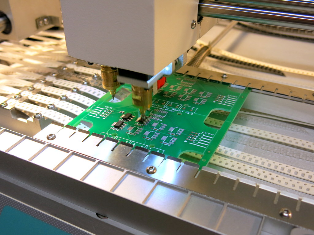
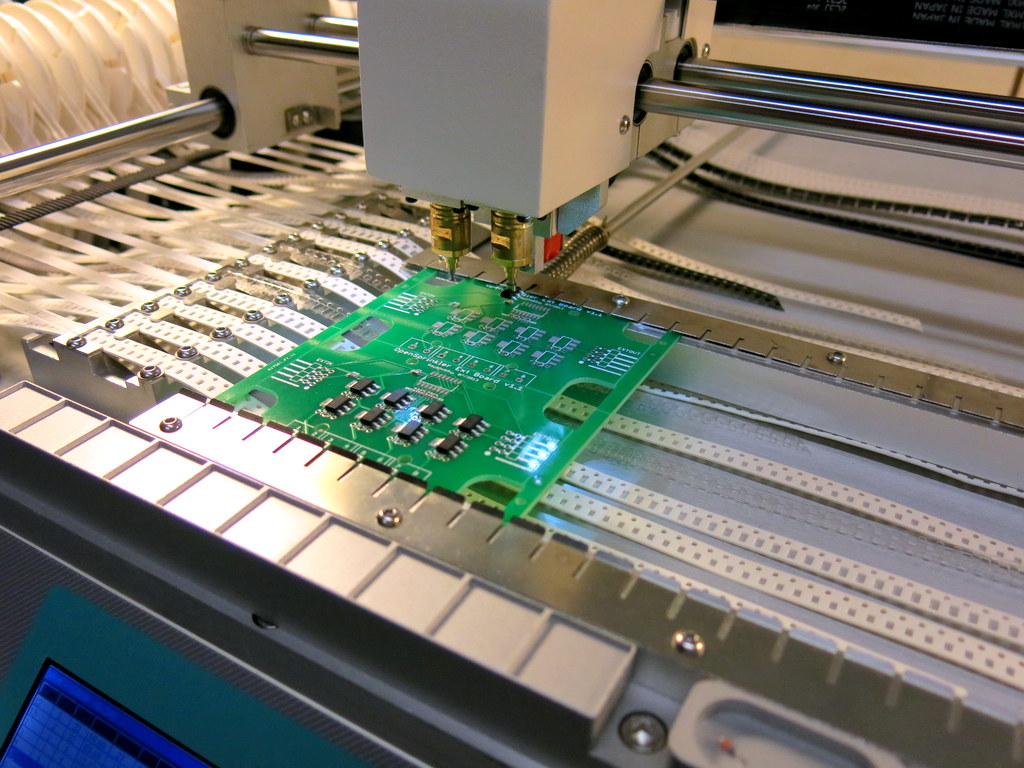
Next step is to populate components. The TM-240A pick and place machine supports PCB panelization. All that I had to do was to open the existing PCB configuration file, and add a new line for each additional sub-board, indicating the amount of shifting from the first sub-board. With this simple change, the PNP machine can now populate twice as many components, a real time-saver!
Here are pictures of four boards before and after reflowing. The reflowing quality is pretty good.

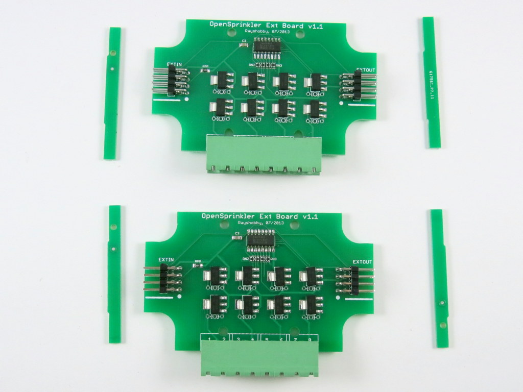
Finally, to separate the boards into individual pieces, as I said, just snap the boards along the V-cuts. Use some strength along the cuts, and they should come off pretty easily. Here are the final results (with the through-hole pin headers and screw terminals soldered in place). Neat, isn’t it 🙂
So, to summarize, it takes very minimal effort to make panelized PCBs. First, when ordering PCBs, tell the manufacturer how you would like to panelize the board. They will do the work for you. Next, order a professionally made solder paste stencil with the PCB order. Finally, modify the pick and place configuration file to reflect the number of sub-boards and the shift amount of each. That’s it. Not bad at all!
