This week I am on a business trip to Shenzhen — the city with the largest electronics markets in the world. My plan is to visit several studios / factories and the of course the electronic markets here, and also some of my old friends. I will try to document my trip as much as I can.
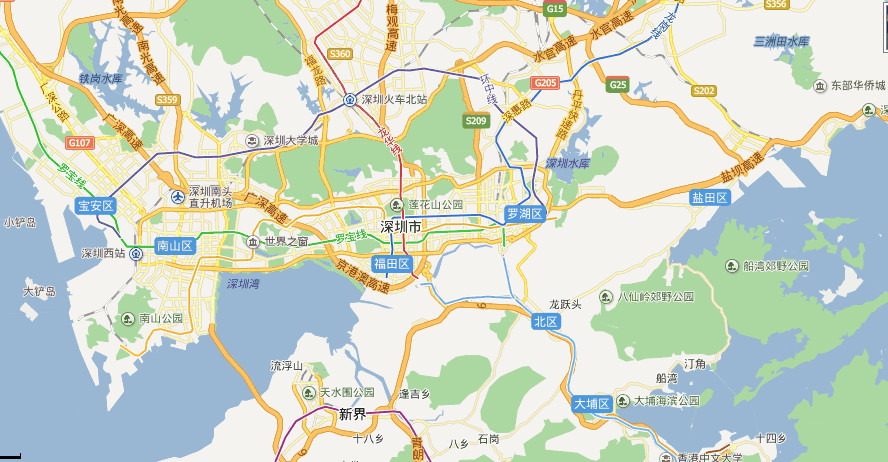

Shenzhen is located at the very south of China — it’s right above Hong Kong. The weather at this season is usually very hot and humid. Fortunately it has been raining for the past couple of days so it’s not as toasting as it normally is. The image above on the right is the look of the city from my hotel window. There is an electronics market right across the street on the other side 🙂
One of the challenges of traveling in China is that a lot of external websites are blocked by the Chinese government. For example, Facebook, Twitter, Gmail, NYTimes. I was able to use a private VPN to get around with it, but the data transfer speed is really slow. On the plus side, you have access to a wide variety of inexpensive food, which is hugely attractive to a gourmet traveler like me 🙂
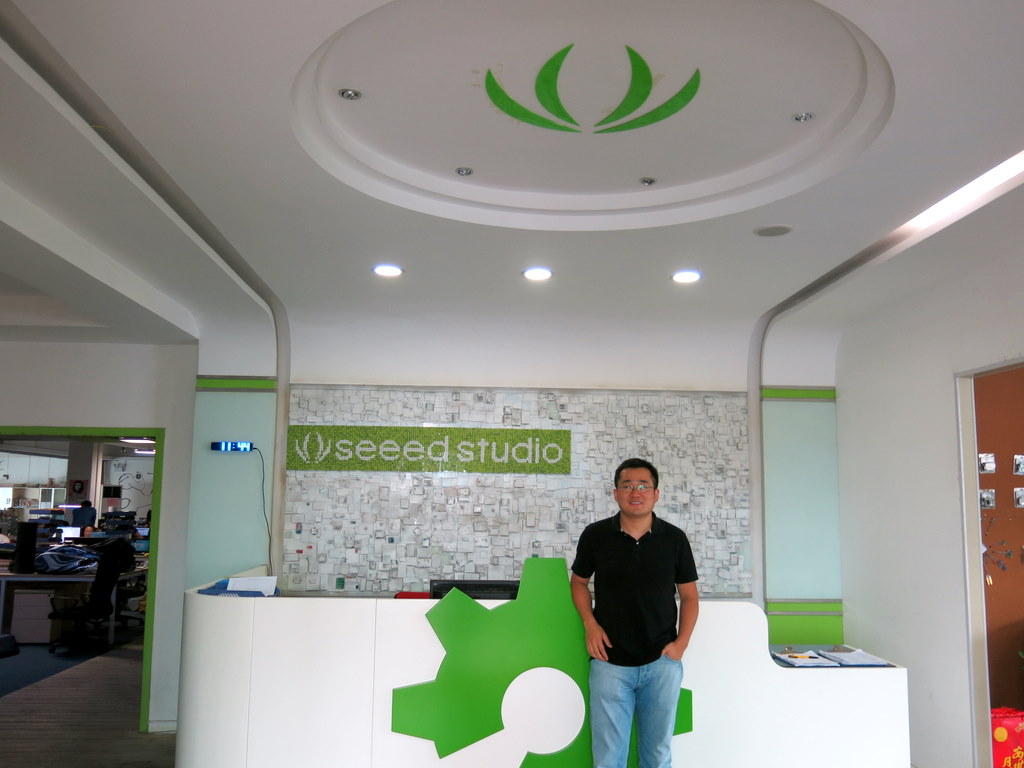
On the first day, I visited SeeedStudio, the company that is currently in charge of manufacturing the fully assembled OpenSprinkler 2.0. SeeedStudio is well known in the open-source hardware community, and they have been growing at amazing speed in the past couple of years. I have been looking forward to this visit for a while.
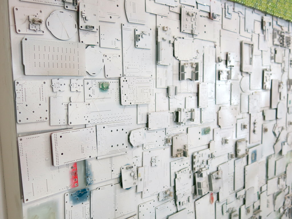
The building where SeeedStudio is located at looks very, short of finding the right word, non-technical, which made me feel that I’ve walked into the wrong place. But as soon as I found their main lobby, I was reassured. On close look, the back wall is made of hundreds of circuit boards painted in white. Very interesting.
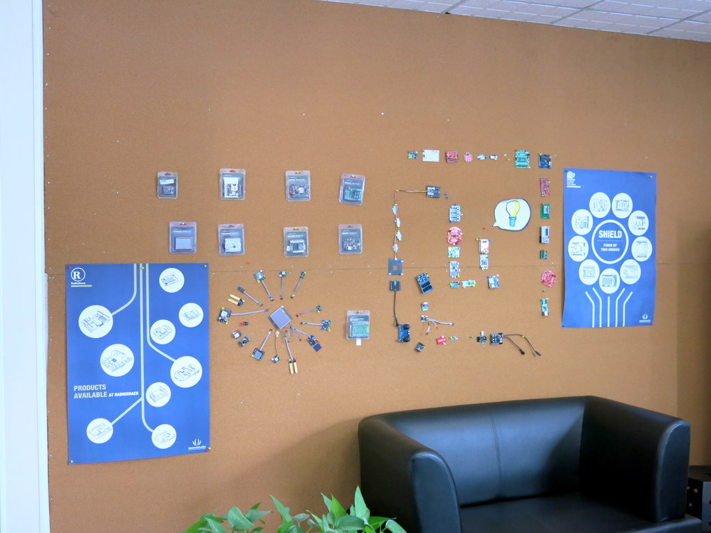
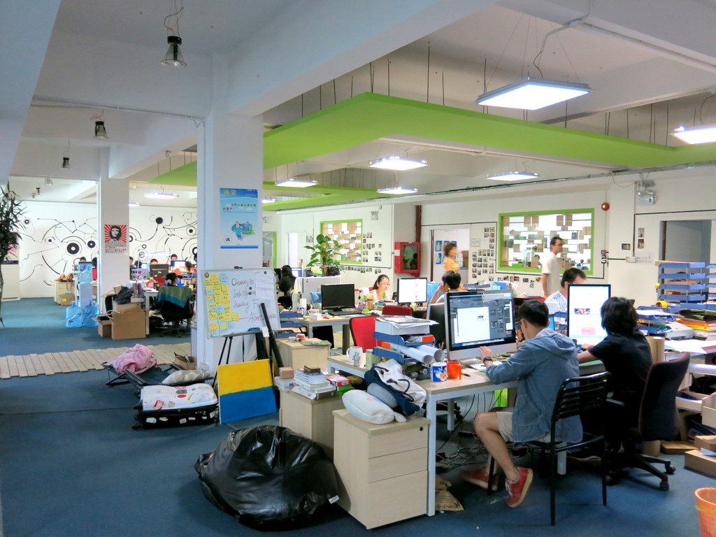
Here is a picture of the ‘innovation corner’ and also the marketing / PR section of the studio.
The main agenda today was to discuss the design of a paper box and a printed user manual for OpenSprinkler, making a mold for the OpenSprinkler Zone Expansion board, and designing a laser cut enclosure for OpenSprinkler Pi. The meeting was quite productive: I talked with the product manager, an enclosure engineer, and an electronics engineer for several hours. Things got started moving right away. Among the electronics discussions, we covered several potential improvements to the current OpenSprinkler circuit, including preventing users from damaging the circuit by inserting the power to the wrong terminal port, automatic detection of defective solenoids, adding built-in WiFi etc. I felt very excited to start prototyping these ideas right away.
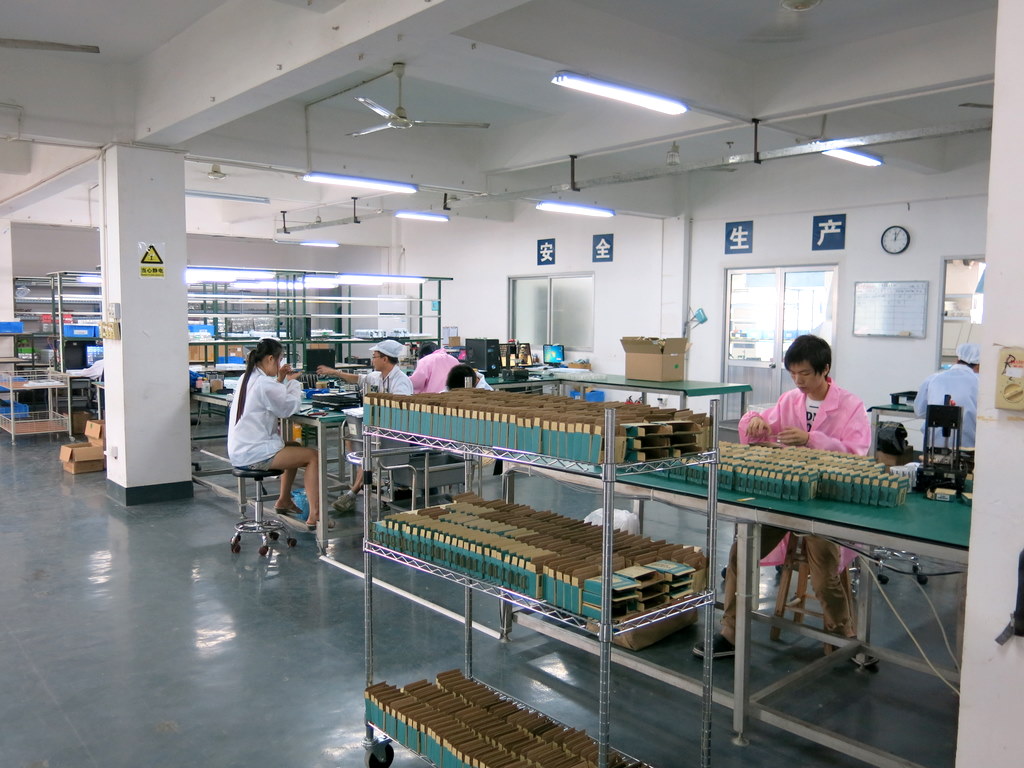
After the meeting, the product manager gave me a short tour of the studio. The top floor is where the offices and meeting rooms are located. The bottom floor is where the production pipeline is.
Here are pictures of the soldering / assembly area, and the SMT pick and place machine.

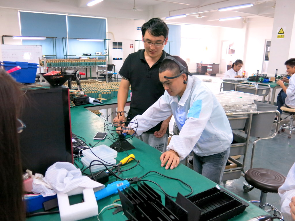
Next, the laser cutter and a testing area where engineers were testing a brain wave (EGG) controlled drones. Hmm, very impressive!

Finally, here are two bins of assembled and tested OpenSprinklers. It really pleases my mind to see these lovely OpenSprinklers 🙂

So that’s all for my report of Day 1. My next stop is Hua Qiang Bei (???), where you can find almost any electronic component you can think of right at the counters. Looking forward to it!
