Feed on
Posts
Comments

24VAC to 5VDC Conversion

Voltage conversion from 24VAC to 5VDC is quite useful, because a lot of home automation devices use 24VAC, including sprinkler solenoids, home surveillance systems etc. Having a conversion module makes it easy to use a single power supply, without a separate 5V adapter for your control circuit. There are plenty of resources you can find online about it. But these resources are rather scattered. So in this blog post I will summarize and discuss the common choices.


AC to DC Rectification

Before we begin, the first step is to have a rectifier that converts voltage from AC to DC. The common choices are half-wave rectifier (which requires just one diode) or full-wave rectifier (which requires four diodes). For simplicity, I will use half-wave rectifier as an example. The typical schematic of a half-wave rectifier is as follows:

half-wave-rectifier

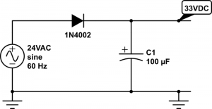
It’s simply a diode followed by a capacitor to smooth out the rectified AC waves. As we know, diode only allows current to flow in one direction, so after the AC voltage passes through the diode, only positive voltage remains. The diode must be selected based on the maximum reverse voltage and the maximum current. One thing easy to forget is that when we talk about 24VAC, we mean the RMS (root-mean squared) magnitude of the voltage is 24V. Since AC voltage is a sine wave, the peak voltage is actually 24 * sqrt(2) = 34V, which is quite a bit higher. The maximum reverse voltage applied on the diode is therefore 34 – (-34) = 68V, which is when the AC voltage runs to the negative peak. So a diode with 70V peak reverse voltage is sufficient.

In practice, transformers that are rated 24VAC usually have a higher no-load voltage, which can vary between 26VAC up to 28VAC. This is typical, and the voltage is supposed to drop close to 24VAC under maximum load (i.e. the current rating of the transformer). As a result, when the circuit is powered on, the transformer can output a peak instantaneous voltage of up to 28 * sqrt(2) = 39.6V.

In the schematic above, I’ve picked a 1N4002 diode (70V reverse voltage, 1A current) and a 100uF/50V capacitor. These should work well for common scenarios. Note that the voltage output on the capacitor is approximately 34V – 1V (diode’s forward drop voltage) = 33VDC. Again, when the transformer is well below maximum load, the output voltage can go as high as 39.6V – 1V = 38.6V.

So next time if you see a power transformer rated 24VAC, after rectification, gives 39VDC, don’t be surprised!!


Now that we have a DC voltage, the next part is to step it down to 5VDC. We want it to be regulated, so that the voltage won’t fluctuate much. There are a variety of solutions:

1. Zener Diode

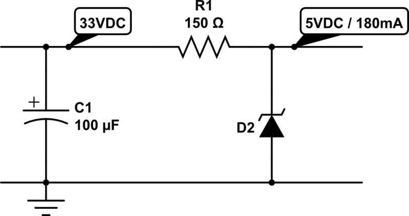
Probably the simplest solution is to use a Zener diode. As we know, a Zener diode can force the voltage across it to remain constant (break-down voltage) when it’s in the break-down condition. This condition is met when the current flowing through it (in reverse direction) is at least a few milli-amps (5mA typical) but less than the maximum current allowed (e.g. the diode’s power rating divided by its break-down voltage). For example, a 5V/1W Zener will remain in break-down condition when the reverse current is between 5mA and 1W/5V = 200mA. The typical schematic is shown as follows:

zener_regulator

Here resistor R1 is used for current limiting. Assume D2 is a 5V Zener diode, and the circuit on the right-hand side draws about 180mA current. R1 must be selected such that the current flowing through it is 180mA plus at least 5mA to keep D2 in break-down condition. So we have R1 = (33 – 5) / 0.185 = 150 ohm. Note that D2 should be rated at least 1W, because in case of open-circuit, it needs to absorb the entire 185mA without burning out.

Now let’s take a look at the power rating of the resistor R1. Since the current flowing through it is 185mA, the power is 0.185 A * 0.185 A * 150 ohm = 5.1 Watt. Wholly crap — this is gotta be a big resistor, isn’t it :). Well, this is the unfortunate drawback of a Zener diode based regulator, that is, it can waste a lot of power and require a bulky resistor. Fundamentally, it regulates the voltage by converting the voltage differential to heat. In this case, the voltage differential is quite big (33V vs. 5V), and the current draw is fairly large (180mA) too, so it ends up wasting a lot of power in heat.

Another drawback is that to increase the current draw, we must decrease R1. Otherwise, if the output circuit starts to draw, say 250mA, that will take D2 out of its break-down condition, and the output voltage is not regulated any more. So overall it is only suitable if the current draw is constant and small (e.g. tens of milliamps).


2. Linear Regulator

Another simple solution is to use a linear regulator, such as the popular 7805. The typical schematic is as follows:

linear_regulator

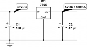
The circuit is quite simple, and the output current can vary across a wider range. However, linear regulator shares the same drawback with Zener diodes, that is, it fundamentally works by converting voltage differential to heat. As a result, it wastes the same amount of energy (5.1 Watt in this case) in heat. This is not only a matter of waste, but also it requires a large heat sink to dissipate the heat, otherwise the regulator will burn and smoke. So clearly not an efficient solution. In fact, the efficiency of a linear regulator is the ratio between the output and input voltages. In this case, it is 5 / 33 = 15.15%, which is very poor.


3. Switching Regulator

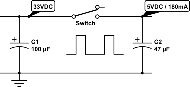
Now we have come to my favorite topic: switching regulator, also known as switching converter, or switch-mode power supply (SMPS). It uses transistors and a reactive component, namely inductor, to convert voltages much more efficiently. Ideally the switching converter works by simulating the following:

smps_ideal

That is, imagine there is an automated switch between the input and output. When the switch is turned on, it connects the input to output, and when it turns off, the input and output are disconnected. This essentially generates a square wave with 33V peak voltage, and the duty cycle is determined by the switch. Suppose the duty cycle is 15.15%, as long as the switching frequency is sufficiently high, at the output it would seem as if you have a constant voltage of 33 * 15.15% = 5V. That’s it, simple!

The main advantage of switching regulator is that since there is no resistive element, theoretically there is no energy loss at all, so the conversion efficiency is 100%! Of course in practice there will be some energy loss due to the imperfections of electronic components. Still, even at 75% efficiency, we are talking about a power waste of only (5V * 0.18A / 0.75) – (5V * 0.18A) = 0.3 Watt, much better than the 5.1 Watt waste you saw previously with a linear regulator.

The schematic above may look very simple. But it doesn’t tell the whole story. Implementing the switch is more complicated than you might think. That brings out the drawback of a switching regulator, namely cost and circuit complexity. It typically involves a transistor or MOSFET that functions as a digitally controlled switch, an oscillator circuit that generates a control square wave, a voltage reference and feedback module that monitors the output voltage, and finally a current sensing or thermal shutdown module that protects the regulator. That’s why switching regulators are typically provided as integrated circuits.

MC34063
Probably the cheapest and most widely used switching regulator is MC34063. The volume pricing (quantity 100+) is only 20 to 30 cents. Dave Jones at the EEVblog has a nice video tutorial about how to use MC34063. Also, there are a lot of MC34063 calculators you can find online, which will help you figure out the component values and parameters.

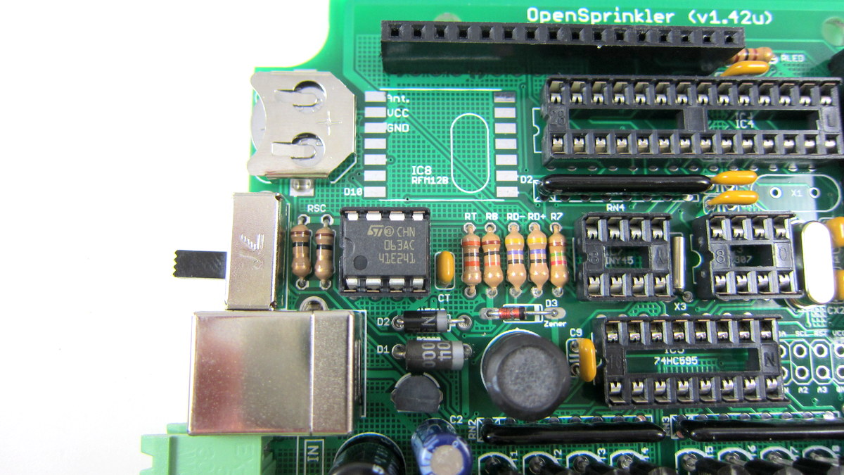
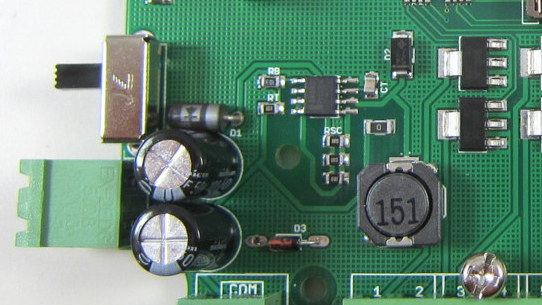
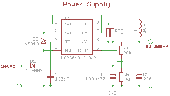
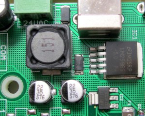
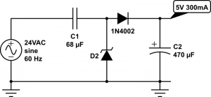
The schematic on the left below shows what I have been using for OpenSprinkler. MC34063 has a maximum input voltage of 40V (and some manufacturers make it 45V), so it’s perfect for our purpose. The main peripheral elements include inductor L1 (150uH), Schottky diode D2 (1N5819), timing capacitor CT (which controls the switching frequency), current limiting resistors Rsc (0.5 ohm), and feedback resistors RT and RB. This circuit can provide 5V 300mA output. The image on the right below shows a picture of the switching regulator section on OpenSprinkler 1.42u DIY kit.

mc34063_schIMG_2627

IMG_2666
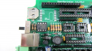
On OpenSprinkler Pi, Rsc is reduced to 0.33 ohm (three 1 ohm resistors in parallel) in order to provide higher current required by RPi. The picture on the left shows the switching regulator section on OpenSprinkler Pi, which uses all surface mount components.

MC34063 is quite flexible. It’s not only useful for step-down voltage conversion, but it can also do step-up conversion (i.e. the output voltage is higher than input voltage), and voltage inversion. On the other hand, it requires a number of peripheral components, and picking the right component values can be tricky, especially if the output current can vary across a wide range. It’s also prone to noise (remember those annoying humming noise from cheap power adapters), and its maximum current is limited to 1.5A.

Overall if you want a cheap switching regulator, and your circuit draws roughly a fixed amount of current well below 1.5A, then MC34063 is a great choice to consider.

LM2596
More recently I’ve started using LM2596 as a replacement for MC43063. I came across it when I was shopping for a modular step-down converter and noticed this one from Amazon.com. LM2596 provides up to 3A output current, requires only a small number of peripheral components, and is more reliable and less noisy. In fact, when I started working on OpenSprinkler, I have used a similar product LM2574 for a while, but that has a current limit ot 500mA, and the switching frequency is much lower.

Here is the new design of the voltage conversion section in the upcoming OpenSprinkler 2.0 and OpenSprinkler Pi 1.1:

lm2596_schIMG_2709

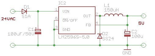
It uses LM2596-5.0, which has a fixed output voltage of 5.0V. The number of peripheral elements is minimal, and the circuit design is very clean. The main downside is that it is considerably more expensive than MC34063. So the extra capabilities don’t come for free 🙂 Still, for reliability and clean design, I have decided to adopt it for all future circuits.


4. Other Solutions

The above has summarized the common choices I’ve learned through my experience. There are certainly other solutions as well. For example, you can use a transformer to step 24VAC down to 5VAC, then from that point on you can use a rectifier followed by a linear regulator to convert it further to 5VDC. This is fairly efficient because transformers can have high efficiency, and the linear regulator in this case is also efficient because the voltage differential is small. However, transformers are bulky and expensive. and this solution is not suitable if the input voltage varies across a wide range.

Another choice is to use a capacitor for current limiting, in conjunction with a rectifier and a 5.6V Zener diode for voltage regulation. The idea is similar to solution 1 above, except it uses the capacitor’s reactance (instead of resistor’s resistance) to limit current. Since there is little energy loss, this is very efficient and is similar to the transformerless power supply design, which is frequently found in small wall adapters. Unfortunately, to provide sufficiently high output current (more than tens of milliamps), you will a capacitor that has high capacitance (e.g. 100uF) and is non-polarized. This is not easy to find in real life.

transformerless_sch

Finally, you may be wondering why not use a resistor-based voltage divider to split 5VDC out of the 33V rectified input? Well, this is a terrible idea in almost any circumstance I can think of. The reason is that the output voltage will fluctuate considerably depending on the current draw. In other words, it is not regulated. So I can’t think of any real use of it other than providing voltage reference.

That’s all. I hope this blog post provides useful information for your own power supply design.


The Cost of Development

During the process of cleaning up my workshop today, I collected all the OpenSprinkler prototype boards that have had design mistakes or were built and failed in the past, and looks at this whole box of lovely PCBs:

IMG_2671

Probably no less than 30 boards in the box. It’s quite shocking to realize how many there are. By far getting prototype PCBs has been the most time-consuming and costly part of the development process. First of all, each round of prototype PCBs costs about $50 and takes 9 to 12 days of lead time (using the fastest shipping option), from places like SeeedStudio or Smart-Prototyping. The cost is not dramatic, but the lead time is quite significant unless if I am willing to pay hundreds of dollars to order from US-based services. Also, these boards are unfortunately complex enough that home DIY PCBs are no longer a viable solution.

Then, no matter how careful I am in designing the PCB, there are always a couple of unforeseen issues that had to be discovered when I actually start assembling. For example, a component might be too far away from the enclosure cutout, a component footprint might be wrong, two components might be too close to each other, the pin headers were placed in the wrong orientation, and sometimes I forget to add a ground plane. Because these issues are only discovered after one round of PCBs have arrived (then I will fix the issues, refine the design, and order another round), they make the development process sequential and cause the overall time and cost to quickly add up. The good thing is that over time I learn from lessons and accumulate tips to help me maximally avoid potential mistakes. Still, it’s inevitable to produce design issues, which can only be fixed by putting in more money and time.

When I get the finalized PCB, however, I often feel proud, as if it’s a work of art which has been refined and polished and is ready to be seen by the public. Then I get a sense of achievement. That’s the joy of working on electronic circuits 🙂

When you are making products in batches, you need a quick way to test them and make sure they function as expected. For example, three weeks ago, I sold close to 100 AASaver kits in a day, and I needed a good way to automate the testing before they are shipped out:

Well, this is what pogo pins are good for. So what is a pogo pin? It’s basically a spring-loaded pin that you can use to make a secure and temporary contact with your circuit board. It allows you to stack the testing circuit directly onto the target circuit, without any additional soldering. The picture on the right above shows an example I got from eBay. This is of model number P75-E, which is 1.02mm in diameter and 16.5mm in length, perfect for the AASaver circuit board.

To build a tester, I need to: 1) provide input power to the target board; 2) test the output voltages (5V/3.3V); and 3) test the output current (>300mA). These can be done by making use of an existing AASaver PCB. I used a total of 5 pogo pins. Two are soldered into the battery holes to provide input power from two AA batteires; two are soldered into the Vcc and Gnd, and further connected to a mini voltage meter for testing output voltages; and one more to provide weight balance. See the pictures below.

To use the tester, I simply stack it onto a target board, and check the voltage readings. Each test can be done in less than 8-10 seconds. To test the output current, I added a 15 Ohm power resistor and a slide switch onto the testing circuit. When the switch is turned on, the power resistor is applied between Vcc and Gnd, which causes an output voltage to drop. This drop should be relatively small (<0.3V) if the target board meets the current rating (>300mA). So there you go: a simple tester for the AASaver!

Recently I was fortunate to receive a Microchip PICkit 2 from Newark.com to write a review on. I was very excited to get it because I have always wanted to learn about PIC microcontrollers. Why? Well, so far I have been quite experienced with Atmel’s AVR family chips, thanks to the Arduino that first got me into electronics. But it’s time to try something new in a new year 🙂 PICs offer several nice appeals including their product variety and functionality (e.g. support for USB, Ethernet, touch sensing etc.) and they have very competitive pricing. I know there are tons of debates about AVRs vs. PICs online. For now I am going to put them aside and make my own comparisons later after I get a good grip of both.

First Impression

PICkit 2 is a very popular tool for programming and debugging Microchip’s PIC microcontrollers. If you want to learn PIC programming, you almost certainly should get one. With the latest device file, it can support most PICs available on the market (although for some of the newer ones it only supports programming and not debugging). Microchip has an updated version — PICkit 3 which supports everything, but I prefer PICkit 2 because it’s cheaper ($34.99) and provides everything I need.

The package (product no. PG164120) contains the programmer itself, two CDs, and a USB cable. The programmer looks very compact. It has a USB port (as well as a key ring) on the top, a red button and three LEDs (power, target, and busy) on the front, and the 6-pin ICSP (In-Circuit Serial Programming) port on the bottom.

Since I am new to the ICSP pins and can easily get myself confused with the AVR’s ISP pins, I made a small label with all the pin names and attached it to the programmer. This way I will never forget the pins when prototyping circuits! The 6 pins are: Vpp, Vdd, Vss, ICSP-Data, ICSP-Clock, and the last pin is unused. Among them, Vpp can provide +12v for high-voltage programming, and Vdd/Vss can supply 5V or 3.3V to power your circuit, which is very convenient. The picture on the right below shows the circuit inside the programmer. It is based on a PIC18F2550 MCU.

At this point I have to say that I like this programmer much better than AVR’s comparable programmer at the same price. Why?

  • I like how the ICSP pins are all on one line. This makes it easy for breadboard experiments as it only needs a 1×6 pin header. In comparison, AVR’s ISP programmer requires a 2×3 pin header, which is always a pain for setting up on breadboard.
  • It can do high-voltage programming, which means if I somehow messed up with the fuse settings I don’t have to panic. In comparison, AVR’s ISP programmer doesn’t do this (unless if you get a more expensive model). I remember the horrible experience when I first programmed my ATMega328 with wrong fuse values, I had to spend a whole day searching for solutions. Eventually I made a high-voltage rescue circuit and fixed the problem. But what a pain!
  • It can provide power (anywhere from 2.5V to 5V) to your circuit.
  • Probably the most valuable of all: it is a programmer and a debugger. You can use it for in-circuit debugging too! How nice! For AVRs, the comparable product would be quite a bit more expensive.

So overall, I am really glad to find out that this small and inexpensive programmer packs a lot of nice features in it.


Software Setup

Next I will try to write my first PIC program. There are basically two pieces of software to install: the MPLAB (version 8.6) which is the programming IDE, and the PICkit 2 standalone program (version 2.61). They are in the attached CDs, but you can also download them online at Microchip’s product website.

The MPLAB integrates everything you need: programming environment, compiler, uploader, and debugger. However, it turns out that it won’t support some of the newer chips (such as the one I got) if you are using PICkit 2. That means you can compile the program but won’t be able to upload it to the chip. The upgraded version PICkit 3 can handle all chips, but I don’t have it! Fortunately, PICkit 2 has a standalone program to work with the newer chips. Be sure to download the latest Device File from that website.

To write a program, you can either use assembly language or use C. I am going with C since I don’t know how to accomplish even a relatively simple program in assembly language. It makes my head blow… Anyway, MPLAB comes with a free HI-TECH C compiler (PICC light version). You can follow the ‘Quick Start’ tutorial, available in the compiler’s installation folder to easily write your first ‘Hello World’ (i.e. flashing LED) program. Here is a snapshot of mine:

The ‘Config’ bits are a bit confusing to me at first. But a read of the microcontroller’s datasheet will make everything clear. These are similar to the fuse settings in the AVRs. The main difference is that here you write the bit settings directly in the program, whereas AVRs separate the program with the fuse settings.


“Hello World” Experiment

For my first experiment, I picked the PIC16F1825 microcontroller. It has 14KB program flash, 1KB RAM, 256B EEPROM, USART, 12 I/O pins, and it costs only $1.50. I thought I made a good choice. Unfortunately soon I found a small issue, which is MPLAB does not fully support this microcontroller if you are using PICkit 2. You can still write and compile a program, but you can’t upload or debug the program (these are only available with PICkit 3). Fortunately, the PICkit 2 standalone program can still work with it. So the solution is to write and compile the program in MPLAB, and use the standalone program to upload:

I made a simple testing circuit, consisting of the microcontroller, a 1×6 ICSP pin header, an LED bar graph and a resistor network. The goal is to, as we always do, flash some LEDs 🙂 The circuit is very easy to implement on a breadboard (see photo above). I basically started by connecting the 6 relevant pins to the ICSP pin header, then all port C pins (C0 through C5) to the LED bar graph, and finally the resistor network. Note that I also attached pin name labels to the microcontroller. In addition to the standard pin names (like A0, A1, C0, C1…), I especially marked the ICSP pins (VPP, ICSP-DAT, and ICSP-CLK). This makes it really easy to connect wires without having to look back again and again at the datasheet.

Upload a program: This is straightforward. First compile the program in MPLAB, then switch to the standalone program, import the compiled HEX file, and click on ‘Write’. The LEDs on the programmer will flash and after a few seconds it’s done.

Power the circuit: As I said earlier, the programmer can supply VDD anywhere between +2.5V to +5V. Note the checkbox for VDD ‘On’ and the voltage input box in the GUI above. Once you enable VDD, the Target LED on the programmer will light up, and the circuit will immediately start running. Voila, my ‘Hello World’ experiment is now complete!


Programming in Linux

I’ve also tried using the programmer in Linux (Ubuntu 11.04). First, MPLAB software installs and works just fine with Wine. Other than the GUI being a bit ugly, the software seems to be fully functional. Second, there is a tool called PK2CMD from Microchip website that works with PICkit2. You can use it to upload a compiled program to your microcontroller. Probably the only missing feature is debugging — there doesn’t seem to be a way to enable debugging in Linux. Well, you can always using MPLAB’s simulator to do software-based debugging. But if you definitely need hardware-based debugging, you can install Windows as a virtual OS in Linux. This way, all features of PICkit2 will be enabled.


Conclusion

So far my first experience with the PICkit 2 programmer has been very positive. It’s small, inexpensive, feature-rich, and relatively easy to use. I highly recommend it. In fact, if you are planning to learn PIC programming, I suggest getting this kit soon. Why? I’ve read from online websites that Microchip is discontinuing this product in favor of the newer PICkit 3, which is pricier and has actually received some negative comments (search for David Jones EEVblog PICkit 3 and you will find out). So before PICkit 2 runs out, go and grab one for yourself!

Resource Links

Finally, there are a few things I am yet to try, and I have put them on my todo list:

  • Try the debugging feature.
  • Program USB — I’ve already got a PIC that has built-in USB support. There are many PICs that have built-in USB and are in DIP package, great for breadboard prototyping.
  • Try USB bootloader.

I’ve had some rudimentary experience with surface mount (SMT) soldering in the past. The method I learned basically involves squeezing out solder paste from a syringe onto the PCB, placing the components, and then using a hot skillet to reflow. It’s pretty easy to learn. But if I want to produce assembled PCBs in large quantity, the syringe method is not going to work well. Instead, I need to use a solder paste stencil to quickly apply solder paste onto PCBs.

Solder paste stencils (aka SMT stencils) are expensive if you want to order them. Even a small piece would cost $30-$40, and that’s often the price for just one. I wanted to learn how to make stencils myself, so I can produce them quickly, and as many as I want. I don’t own a laser cutter. Fortunately, I found this really clever method from Instructables. After trying it a couple times, I’ve got a good grip of it. Below I document the process with pictures. The method is essentially based on the Instructables article above, but combined with my own experience and tips.

Preparation

To begin, you need thin copper sheet. The thickness of the copper sheet should be around 3 to 4mil (0.003 to 0.004 inch). I got mine from Amazon: 12 inch by 12 inch for a reasonable price. Use scissors to cut a small piece from the sheet. The size should be twice as large as the actual PCB size, to avoid solder paste from running off the stencil.
Clean the copper surface using some Bar Keepers Friend.
Now use a laser printer to print the color inverse of the top stencil mask onto a piece of magazine paper. Use the highest toner darkness. The color inverse means you want the stencil masks to be white, and the rest to be black. After etching, the solder masks will become holes in the sheet, thus creating a ‘stencil’.
Now use the toner transfer method to transfer the print to the copper sheet. There are many online instructions for the toner transfer method, but according to my experience, the following two tips make it really a breeze. 1) Use magazine papers for the printout. Don’t use glossy photo papers — they are expensive and difficult to peel off. Magazine papers work like a charm. 2) Use a GBC laminator for transfer. It’s much, much easier (did I say much?) than a hot iron. Place the printout face down on the copper sheet, and run it through the laminator at least 10 times. Then throw the copper to hot water. After 5 minute you can peel off the magazine paper. Really easy.

Etching

The next step is very important: you need to cover the bare copper surfaces with tape. This includes both the front and the back sides. You don’t want them to be etched out. Of course the tape should not run too much into the region of the printout — you don’t want to cover any solder mask holes that should be etched out.
Now it’s time to throw the thing into an etchant and let the exposed copper be etched out! Instead of Ferric Chloride, I like using the fast solution that consists of one part muriatic acid + two parts hydrogen peroxide. Very cheap in terms of material cost, and very effective. You can get muriatic acid from Lowes. Just be careful: do not let your skin touch it, and do not breath it directly.
After etching is complete, carefully remove the tapes. Then use Acetone to remove the black toner. Finally, polish the copper surface with a Scotch-Brite scrub sponge. Voila, the solder paste stencil is done! Looks quite pretty.

If you are experienced, the whole process should take no more than 40 minutes. You can make as many stencils as you want. I haven’t tried making a stencil with really small component footprints. I will try that at some point and see how accurate the stencil can be.

Apply Solder Paste

Now it’s time to see some stenciling in action! First, use three spare PCBs to make a tight frame, and insert the target PCB into the frame.
My target PCB today is the AASaver / Breakboard Power Supply. This is a little boost converter that bumps a voltage as low as 0.8V to 5V or 3.3V, which can be used to power bright LEDs or serve as breakboard power supply.
Carefully position the stencil on top of the target PCB, and align the holes with the solder pads. After you are satisfied with the alignment, use a tape to fix the left edge of the stencil. This way, you can easily life the stencil up when you are done, and you don’t have to re-align for the next PCB.
The next step is to apply the solder paste. This is a bit nasty. You need to prepare a putty knife (available in home improvement stores) and some solder paste. I got my solder paste from DealExtreme.com. Cheap and works really well (the only downside is the long shipping time).
I didn’t make a video to show how to apply the solder paste. Fortunately, Sparkfun electronics has a great video tutorial which I included on the left. Check it out!
This is the outcome of applying solder paste to nine PCBs. Click on the image to see a zoom-in view. It’s really fast.

Place SMT Components


Placing SMT components onto the PCB is often the trickiest step. These kids are so tiny that even a small breath from your mouth will blow them away. Not only are they difficult to hold still, but it’s tricky to get them out from their packages.

But don’t worry, I found a good way to hold them still so they won’t get lost easily. The method is very simple. Just use some magnets! Most SMT components attract well to magnets. You can 1) easily dump components from their packages to the magnetic surface, and 2) move or even lift up the magnets, and the components won’t fall off. So next time when you travel, don’t forget to buy some extra magnets!

Use tweezers to carefully move components from the magnets to the PCBs, and place them in the right spots. Here is the outcome of SMT placement.

As some point I will need to buy a pick and place machine to automate this step.

Hot Skillet Reflow


Now it’s time for some hot skillet action. Place several component populated PCBs into an electric skillet. Turn to the maximum power. In about 2-3 minutes the reflow will start to happen. As soon as it’s done, turn off the power and let the PCBs cool down. If you’ve never done the reflow before, check out Sparkfun’s awesome Reflow Skillet tutorial.

You should do this outdoors because the fumes produced during reflow are toxic, and you certainly don’t want to breathe them! The picture on the left shows the outcome of the reflow.

Lastly, perform careful visual checking to see if every component is soldered properly. Also do a basic electric test to see if the circuit functions correctly.

The Final Result

Here you are, a fully functioning AA Saver / Breakboard Power Supply! I will write another blog article shortly to introduce this small yet very useful circuit. Stay tuned.

« Newer Posts - Older Posts »