Exciting news! We’re gearing up to launch a new hardware revision of the AC-powered OpenSprinkler: introducing version 3.4 — a sleek, refreshed take on the ESP8266-based OpenSprinkler. While it retains the same familiar circuit as the current v3.3, version 3.4 features a completely redesigned enclosure for a refreshing new look. Check out the sneak peek photos below!
TL;DR – What’s New in OpenSprinkler v3.4:
- Single-layer circuit – Replaces previous 2-layer design to reduce assembly time and cost
- Revised enclosure size – Lower profile and adjusted dimensions due to circuit layout change
- Two extra sensor ports (SN3, SN4) – Added to standardize parts and simplify sourcing
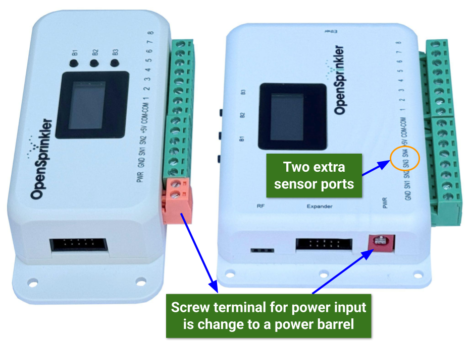
- Switched to power barrel jack – Easier power adapter hookup, no wire stripping required
- Added external Ethernet connector – Simplifies wired Ethernet module installation
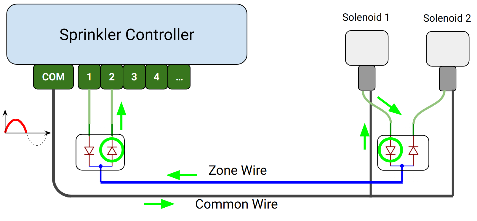
The most significant update in version 3.4 is the shift from a two-layer circuit design—consisting of a top logic board and a bottom driver board—to a streamlined single-layer layout. Originally, the two-layer design in OpenSprinkler v3 was introduced to support interchangeable driver boards (AC-powered, DC-powered, and Latch), allowing the same logic board to interface with various solenoid types. While this approach offered flexibility, it also made assembly more complex and time-consuming. In version 3.4, we’ve consolidated the design into a single board, significantly simplifying assembly and improving overall efficiency.
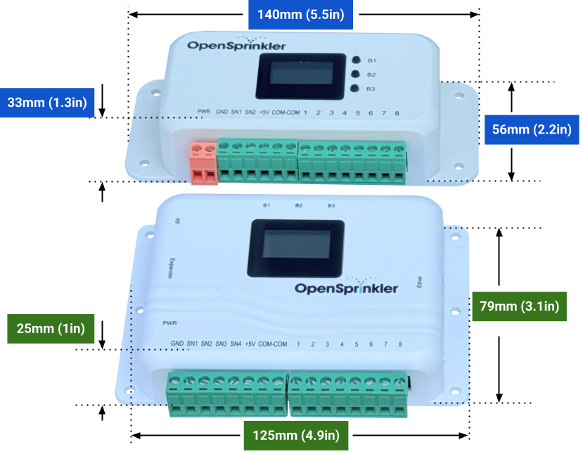
As a result of the single-layer layout, the enclosure height is noticeably reduced: from 33mm (1.3in) to 25mm (1in). The length is slightly reduced, and the width is moderately increased from 56mm (2.2in) to 79mm (3.1in).
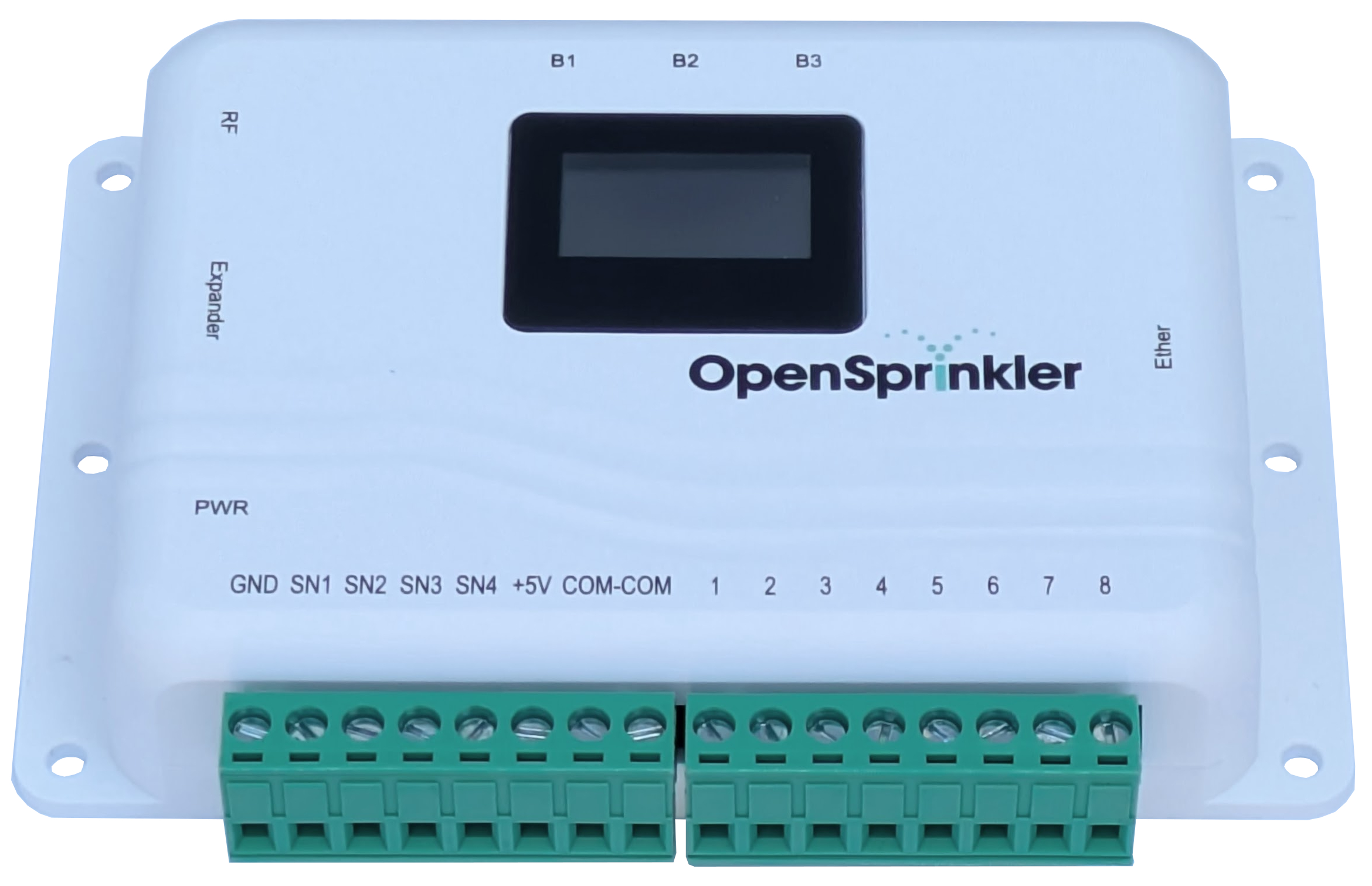
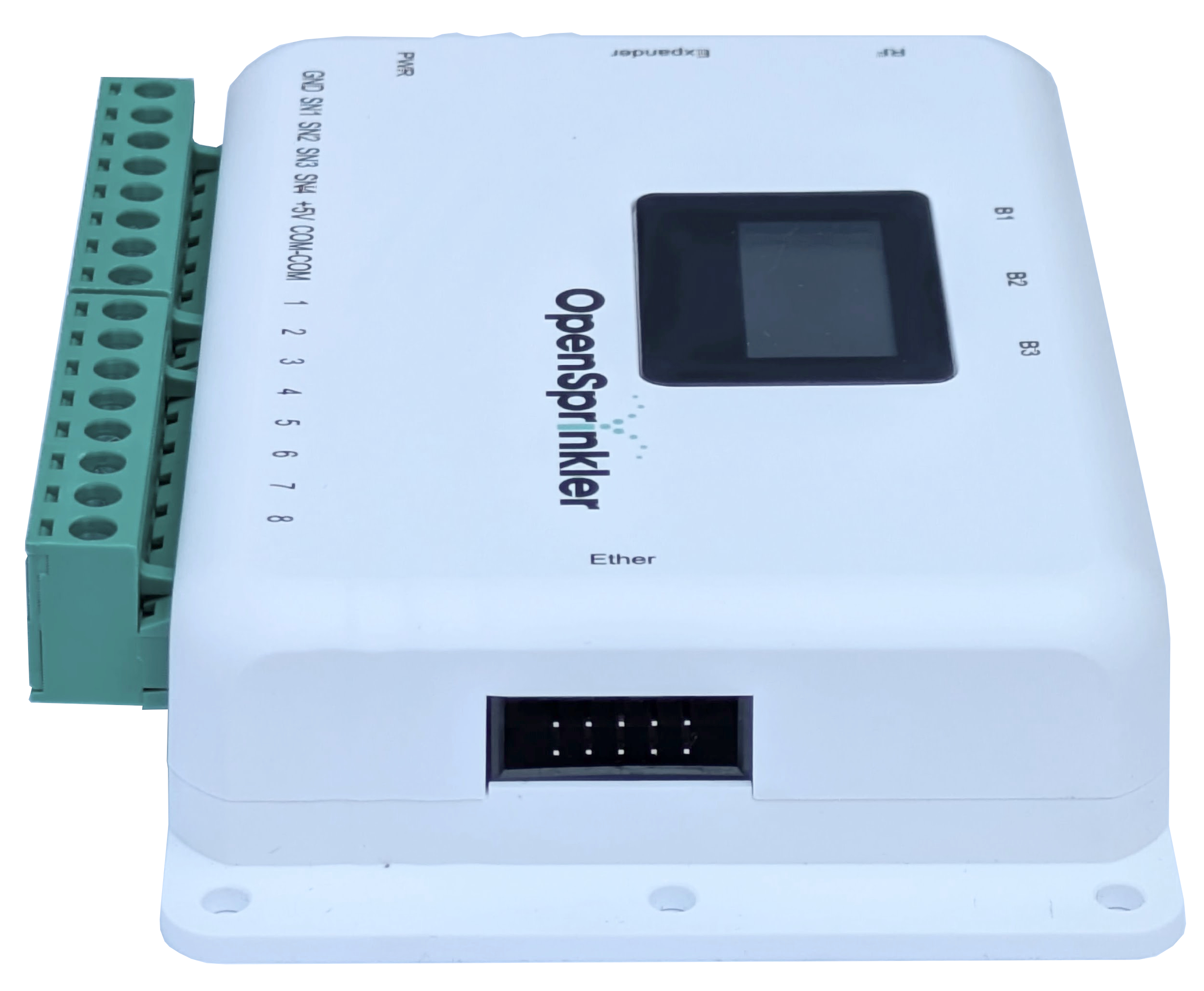
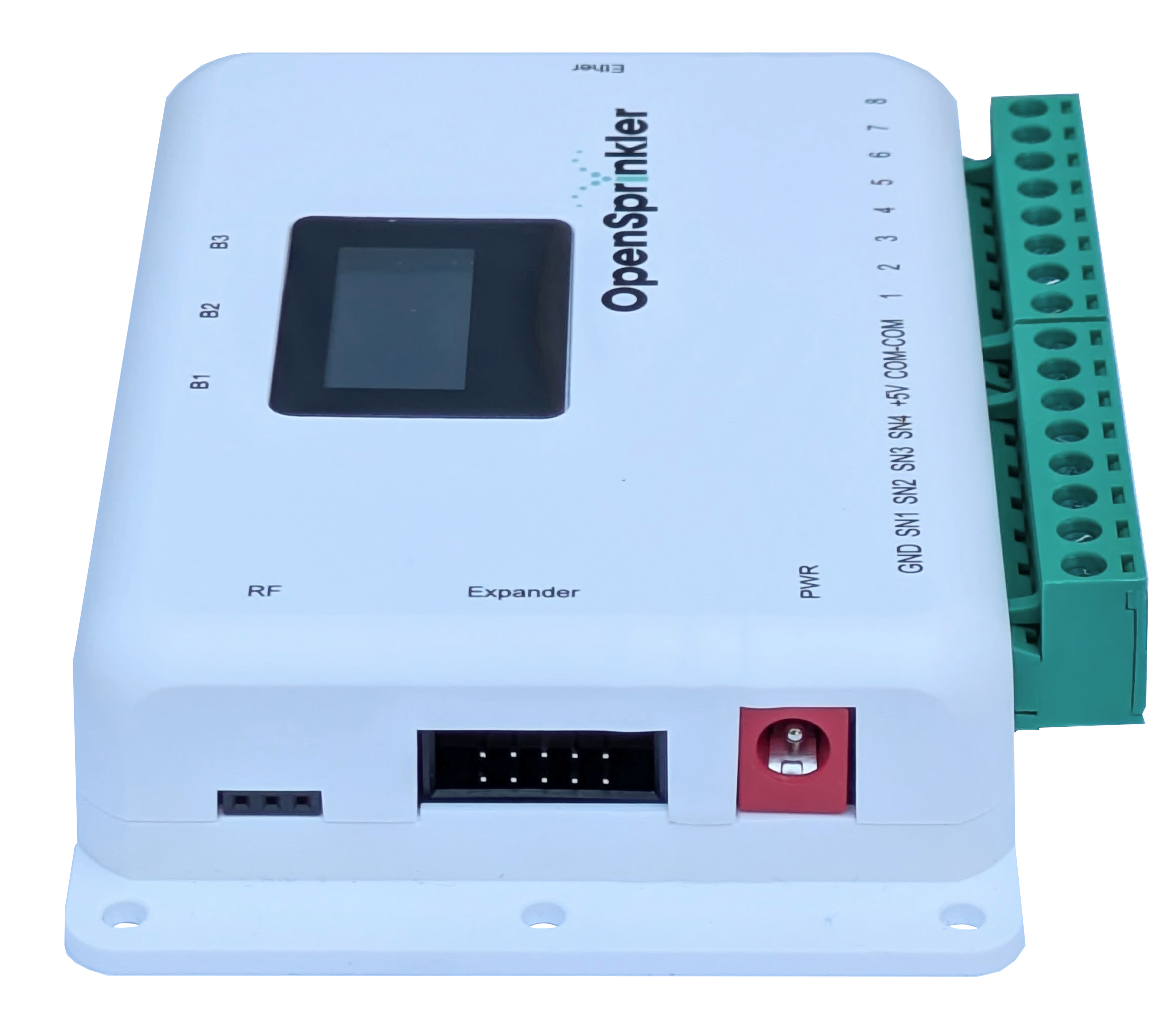
The circuit design in version 3.4 remains largely unchanged from v3.3. However, one notable enhancement is the addition of two new sensor ports: SN3 and SN4. This upgrade is driven partly by the aesthetics of the new enclosure and partly by the decision to use the same 8-pin terminal block as the zone ports. This simplifies part sourcing and reduces inventory management overhead. Initially SN3 and SN4 will be inactive, and they will be enabled in a future firmware update.
Another improvement is the change to the power input port. The current orange 2-pin terminal has been replaced with a red-colored power barrel connector. Since most 24 VAC power adapters—including the one we provide—come with a standard plug, this change allows users to plug in power directly, eliminating the need for using an adapter cable or stripping wires, which has been a common pain point for some users.
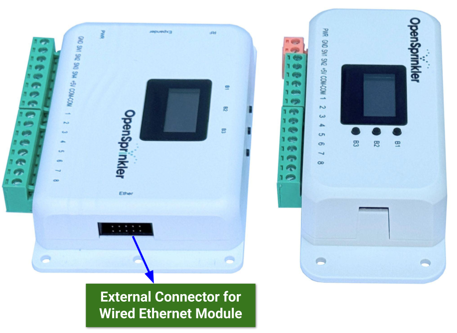
Finally, an external connector for the wired Ethernet module has been added to the right side of the enclosure, making installation much more convenient. Previously, the Ethernet connector was located on the internal circuit board, requiring users to open the enclosure, plug in the cable inside, and route it through a small opening—a process that was quite cumbersome. You see, when OpenSprinkler v3.0 was first introduced, I didn’t plan to have wired Ethernet as ESP8266 already provided built-in WiFi. But in response to strong user demand, I improvised a solution by adding an internal connector and repurposed an opening—originally intended for a now-removed RF receiver—to route the cable outside. While the workaround was functional, it was far from ideal. With version 3.4, the enclosure finally includes a dedicated external connector, making Ethernet installation simple and user-friendly.
Below are side-by-side comparisons of v3.3 and v3.4:
Other Questions You May Have:
Q: When will it be available?
A: We’ve started accepting pre-orders for OpenSprinkler v3.4, with shipments expected no later than mid-July 2025.
Q: What are the exact dimensions of the v3.4 enclosure compared to v3.3?
A: The new enclosure (v3.4) measures 125mm (L) × 79mm (W) × 25mm (H), or 4.9in × 3.1in × 1in. For comparison, the v3.3 enclosure is 140mm x 56mm x 33mm, or 5.5in x 2.2in x 1.3in.
Q: What about OpenSprinkler DC and Latch models?
A: Version 3.4 of the DC and Latch models are in development and expected to be ready by August November 2025. Until then, we’ll continue selling version 3.3 of these two models. The new models will not only feature the updated enclosure, but switch to a USB-C power adapter for better availability and ease of use.
Q: Which expander is it compatible with?
A: OpenSprinkler v3.4 is fully compatible with Expander v3, just like previous v3 controllers. If you already own Expander v3, it will continue to work seamlessly.
Q: Will version 3.3 still be available?
A: Yes, temporarily. We’ll continue selling v3.3 while supplies of its enclosure last. After that, we plan to offer v3.3 circuit boards without enclosures for repair purposes and DIY projects. We’ll also provide 3D design files for the v3.3 enclosure so users can print or order the enclosure as needed.
Q: Will version 3.4 require different firmware?
A: No. All OpenSprinkler v3 controllers use the same firmware. The system automatically detects the hardware version and make software adjustments accordingly.
Q: Can I use my existing wired Ethernet module from v3.3?
A: Yes. Version 3.4 uses the same W5500 Ethernet module as v3.3, so it remains fully compatible.
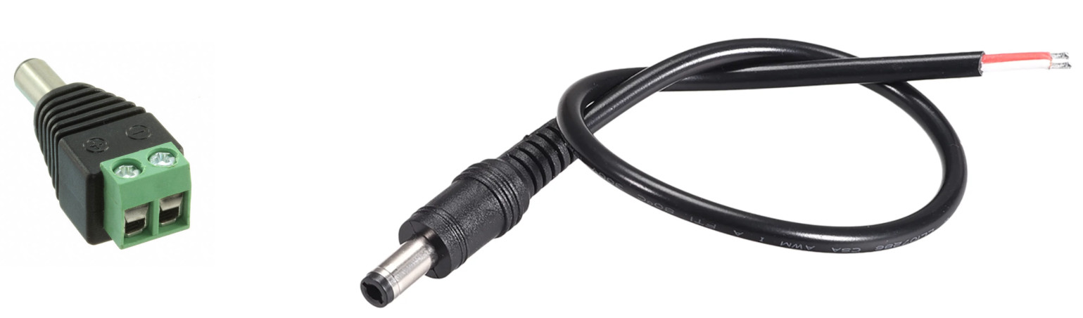
Q: I have an existing 24VAC power adapter with stripped wires. Do I need a new adapter?
A: Not necessarily. You can use a plug adapter to convert the stripped wires into a standard male barrel plug. Here are two common options: (the search terms are “power jack plug adapter” or “power pigtail barrel“).
Q: I just bought an OpenSprinkler AC v3.3 recently. Can I exchange it for v3.4?
A: Yes, as long as your purchase was made within 30 days, which qualifies under our no-questions-asked return and refund policy (see our terms and conditions). Please note that in terms of functionality and circuit design, v3.3 and v3.4 are nearly identical, aside from the two additional sensor ports on v3.4.