We are happy to announce that OpenGarage firmware 1.2.0 is now officially available. The main change of this firmware is on cloud connection options for remote access: it now supports both Blynk and OpenThings Cloud (OTC) connections. Previous firmwares have only supported Blynk. The motivation for this change is the fact that the Blynk team is officially ending the Blynk legacy app and legacy server; in the meantime we have developed our own cloud proxy called OpenThingsFramework. So it’s the right time for us to push out our own cloud framework.
What are the technical differences? With Blynk, data is stored on the cloud server, which serves as a ‘cache’ between the application and firmware. In contrast, OpenThingsFramework is a proxy — it does not store data on the cloud server, instead, when a request comes from the application, it’s forwarded directly to the firmware, which sends responds back. This is implemented using WebSocket and persistent TCP connection. There are pros and cons of each approach. For example, Blynk has a faster response time, since the data is ‘cached’ on the cloud server; however, the firmware design is more complicated as the built-in web interface of OpenGarage cannot be easily replicated using Blynk. Also, some users may have privacy concerns over data stored on the cloud server. With OpenThingsFramework, data is never stored on the cloud server; and its proxy nature allows the same built-in web interface to be remotely accessible. This significantly simplifies the firmware design: only a small number of changes are needed in firmware code to allow remote access. On the other hand, the response speed can be slow, since the server does not ‘cache’ any data.
Both Blynk and OTC options are supported by our OpenGarage mobile app, as well as a simple OpenGarage web app that I wrote. To users, the practical differences are as follows: push notification is only available with Blynk, and you must have the Blynk legacy app installed on your phone. This legacy app is no longer available in the app store (since the Blynk team has discontinued it). However, if you are Android user, you can still find and install this app manually. That said, you can always use IFTTT for push notification, which is independent of either Blynk or OTC. If you need the ability to remotely access the full built-in user interface of OpenGarage, including changing settings and viewing log data, only OTC supports it. Otherwise, if you just need the ability to check door status and car status, and trigger door actions remotely, you can go with either of them. Please note that as the official Blynk server is going offline soon, if you want to use Blynk, we recommend you to create your Blynk token on our own server at openthings.io. The support article here explains how to create and use Blynk and OTC tokens respectively. I’ve also created a new OpenGarage video that gives you a quick walk-through of the steps. The section starting at 7:25 is about cloud tokens:
If you decide to upgrade to firmware 1.2.0, please note that it requires ESP8266 WiFi chip that has 4MB flash. Most OpenGarage units sold in recent years have 4MB flash, the only exceptions are the early versions (v1.0, 1.1 and 1.2 I believe). Also, as this firmware has changed the flash memory layout, it will trigger a factory reset so it will lose all settings and WiFi configuration. You will need to reconfigure WiFi after the firmware update. Finally, you can choose to use either Blynk or OTC, but you can’t use both of them at the same time.
This post documents some of the tips and tricks I learned while integrating ESP8266 into my own circuit designs. Some of them help reduce the components needed thus minimizing the cost, while others have to do with selecting and using GPIO pins. For breadboard prototyping, you can certainly use one of the popular ESP8266 development boards, like NodeMCU, WeMos etc. But what I want to cover in this post is to integrate a ESP8266 module (such as ESP-12F) into the circuit design, without using the development boards.
In the past several years, I’ve gradually transitioned all my gadgets from using the classic ATmega chips (including ATmega328 and ATmega1284) to ESP8266. There are a lot of advantages of ESP8266: it has built-in WiFi, it’s Arduino compatible, it has a lot more RAM and flash memory space than the classic ATmega chips, and it’s really cheap. In fact, due to the ongoing chip shortage, the ATmega chips have become more expensive and difficult to source, while ESP8266 is still widely available at a very cheap price. ESP8266 certainly has some downsides as well: it has a relatively small number of GPIO pins, particularly, it has only one analog pin, which limits its applications; also it can be tricky to use in low-power applications driven by battery power. Nonetheless, as most of my gadgets are powered by USB (+5V), ESP8266 is a perfect choice for me.
Power Circuit
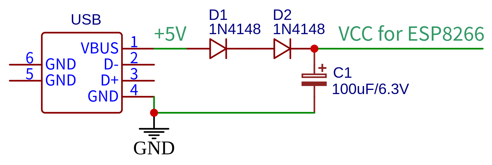
The operating voltage range of ESP8266 is 2.5~3.6V, with 3.3V being the most common. If the input voltage is 5V (from USB), a common method is to use a 3.3V linear voltage regulator, such as AMS1117-3.3. At first, I thought that pretty much any jellybean 3.3V regulator would be sufficient. However, it turns out that ESP8266 can draw a fairly large amount of surge current instantaneously, so some cheap regulators I’ve tried, such as XC6206-3.3V, does not work reliably at all, even though on paper it claims to handle a maximum current of 250mA.
Now, from 5V to 3.3V there is a 1.7V voltage drop, which is about 2 diode drops. Realizing this, I found that a very cheap and quite reliable method to provide power to ESP8266 is to simply use two 1N4148 diodes in series. Under the typical current draw of ESP8266, each diode drops about 0.75~0.85V; with two of them in series, the voltage comes out to be almost exactly 3.3V. Also, as diodes can handle instantaneous current surge quite well, this method works quite reliably, compared to some of the weak voltage regulators.
On the output of the two diodes, you do need a 100~220uF to provide a sufficient buffer. However, since the voltage is low (~3.3V), the capacitor isn’t necessarily large in physical size. A 100uF electrolytic or tantalum capacitor rated at 6.3V or 10V should work just fine. The schematic below shows this simple power circuit.
Two diodes in series provide the required voltage drop
Note the assumption is that the input voltage is from a +5V USB power source, which can provide a minimum of 500mA stable output current. This is indeed the most common case for me. If the input voltage is much higher than 5V, you will still need a voltage regulator. In fact, if the input voltage is significantly higher than 5V, you likely will need a switching regulator for efficiency reasons.
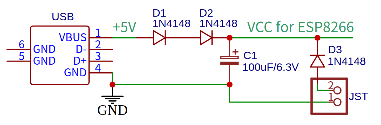
I’ve also had several cases where the gadget need to be powered from USB as well as a lithium battery. The above diode-based power circuit can be easily extended to support dual power sources, as shown below.
Diode D3 both provides voltage drop and blocks reverse current
Here JST is a lithium battery connector. Diode D3 provides the necessary voltage drop: a standard single-cell lithium battery gives 3.7~4.2V, so after D3 it becomes 3~3.5V, which is within the operating voltage of ESP8266. D3 also blocks reverse current in case both USB and lithium battery are plugged in at the same time. This way, at any given time, only one of the two sources will be automatically selected to provide current to ESP8266.
This circuit can also be extended to support charging of lithium battery through USB, such as by using the popular TP4054 battery charger. The input of the charger is 5V from USB, and output is pin 2 of the JST connector. This way, the lithium battery can be connected at all times, and it will be charged whenever USB is plugged in.
Auto-Reset Circuit
A very convenient feature of ESP8266 development boards is the auto-reset circuit: when programming ESP8266, the auto-reset circuit triggers the bootloading sequence automatically before sketch uploading starts, thus there is no need to press any button to manually enter the bootloading mode. This is accomplished by toggling pins on the USB-serial chip with appropriate timing sequence, to simulate a reset while GPIO0 is being held low.
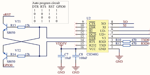
Using CH340 (a very popular, low-cost USB-serial chip) as example: the typical auto-reset circuit such as used on NodeMCU, is as follows:
The auto-reset circuit on NodeMCU
Here the DTR and RTS pins on CH340 are connected to the auto-reset circuit involving two resistors and two NPN transistors. My understanding is that the two transistors are essentially level-shifting circuits, because in the schematic here, CH340 operates at 5V, while ESP8266 operates at 3.3V.
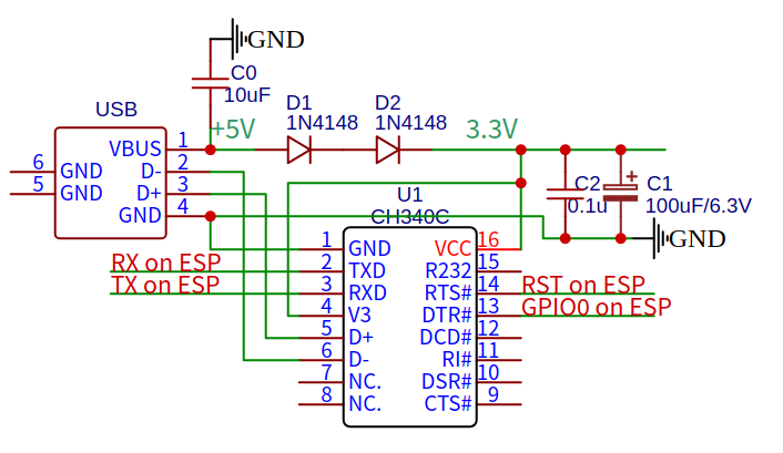
However, CH340 can operate perfectly fine under 3.3V. So if we power CH340 and ESP8266 both with 3.3V, then there is no need to use the level shifting circuits, saving two resistors and two transistors. Below is my simplified auto-reset circuit:
Simplified auto-reset circuit, without level shifting
Note that this circuit uses the CH340C variant of the CH340 chip (there are several variants: G, C, B, T, etc.) because it has built-in 12MHz oscillator, thus there is no need to connect an external crystal oscillator. Also, note that the V3 pin is connected to 3.3V, this is required if it’s CH340 is powered by 3.3V. The TXD, RXD, RTS, and DTR pins on CH340 are connected to RX, TX, RST (Reset) and GPIO0 pins on ESP8266 respectively. No more NPN transistors for level shifting.
GPIO10 comes handy when you really need one more GPIO
If you are familiar with ESP8266, you are probably aware of the typical set of available GPIO pins. These are:
GPIO0: the bootloading indicator pin, usually pulled high, can be used as a button if needed.
GPIO1/3: the default TX/RX pins, generally connected to the USB-serial chip as above.
GPIO2: connected to the built-in LED on ESP12-F, active low. Must be pulled high at booting.
GPIO4/5: the default I2C pins. I generally use them for connecting to I2C components like SSD1306 OLED display, real-time clock etc.
GPIO12/13/14: general-purpose IO pins that are good for anything; support interrupts and internal pull-ups. These are also the hardware SPI’s MISO, MOSI, and SCK pins, so you will need them if you have SPI components like Ethernet modules, external SD card etc.
GPIO15: must be pulled low at booting. Because this pin is guaranteed to be low at booting, it’s suitable for connecting to output components like a relay, a buzzer, an LED etc. which should be inactive at booting. This is also the hardware SPI’s CS pin, but you don’t have to use it as CS — you can use any GPIO pins as CS pin for SPI.
GPIO16: this is a restricted pin that does not support interrupt, and has internal pull-down resistor instead of pull-up as the other GPIOs. Other that these restrictions, it can be used as either input or output, but it does have glitches at booting, as detailed below.
As you can see, the number of GPIO pins is quite limited, and those that are truly flexible (i.e. no restrictions and no HIGH/LOW requirements at booting) is even more scarce. What if you just need one more pin? After searching around, I discovered that GPIO10 is another all-around good GPIO pin that you can use. This pin is often not discussed because it’s connected to the internal SPI flash and thus can be problematic to use as GPIO. However, it turns out that this pin is totally usable as long as you make sure the flash mode of ESP8266 is dio (i..e NO qio or qout mode: they will cause GPIO10 to be unusable). Other than that, you can use GPIO10 as input or output, it supports interrupt and internal pull-up.
Some of the forums also mention GPIO9: unfortunately this doesn’t seem to be usable at all. I’ve tried and it always gets my ESP8266 stuck so I gave up.
If you need a lot more GPIO pins, check out my previous post about IO expander chips — it talks about different IO expander options and their pros and cons.
Using a GPIO pin to indicate hardware revision
Occasionally I make changes to a circuit, which often involves re-assigning GPIO pins for different components. For example, in the initial version of a circuit, I assigned GPIO15 to a buzzer; then in a later revision, I ended up removing the buzzer and re-assigning GPIO15 to the CS pin of an Ethernet module. With these different hardware revisions, it’s necessary to also make firmware changes. But I don’t want to maintain so many different versions of the code. Instead, I want the same firmware to automatically detect which hardware revision it is. A common trick I’ve used is to dedicate a spare GPIO pin for this purpose. The way this works is that all GPIO pins on ESP8266 have internal pull-ups (except GPIO16, which has an internal pull-down and not up). The resistance on these pull-ups (or down) is about 40 to 60 Kohm. So assuming nothing is connected to a pin, if you turn on the internal pull-up, it should read HIGH right after booting up. To indicate a different hardware revision, you can connect the pin with a resistor to ground (the resistor value can be anywhere between 1~10 K). This way, the pin will read a LOW even as internal pull-up is enabled. This can be used as an indicator for a different hardware revision.
Of course the downside of this method is that it sacrifices a GPIO pin. But some pins, like GPIO16, has some restrictions that make them less useful than other pins, so why not dedicate it as a revision indicator 🙂
Getting Rid of CH340
So in the above I’ve just talked about how to simplify the auto-reset circuit to save two resistors and NPN transistors. Now, if I am planning to stay with OTA (over-the-air) firmware update, that is, update firmware through WiFi only and not through USB, then I can even get rid of the CH340 USB-serial chip, saving one entire chip from the circuit design! But wait a minute, I still have to program the initial firmware, so I still need a way to use an external USB-serial adapter to do so!
This can be done by one of several common approaches: for example, you can solder a pin header to the circuit to allow plugging in an external USB-serial adapter; if you don’t even want pin headers, you can get rid of them by using a programmer with pogo pins that, when pressed down, can make temporary contact with the circuit. Along that line, I’ve also made dedicated 3D-printed programming assemblies like in the pictures shown below:
Left: a USB-serial programmer with pogo pins; Right: a 3D-printed assembly with pogo pins.
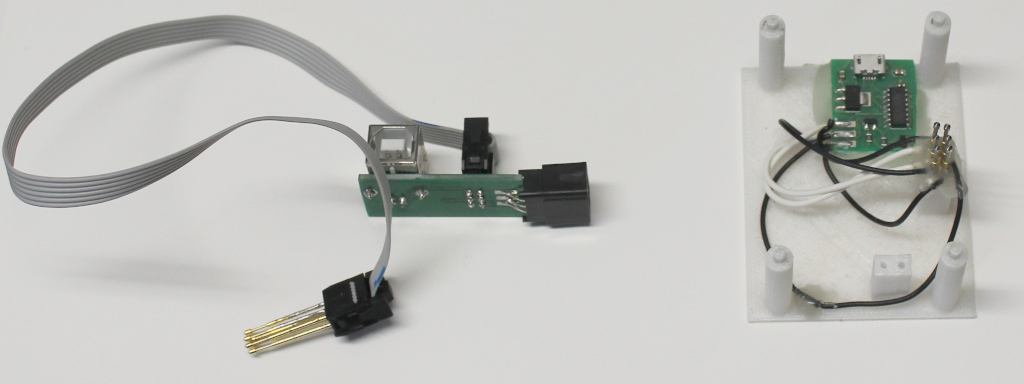
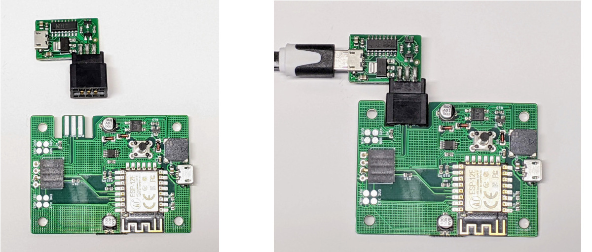
After experimenting with various methods, my favorite one at the moment is to use a card-edge connector that can directly plug into the circuit board. This is basically like the pin-header approach but without having to solder anything. Specifically, I made a custom programmer with CH340 and a 2×3 card edge connector. Then on the circuit board containing ESP8266, I make a matching section, using cutouts and SMD pads, to plug into the connector of the programmer. Standard PCB thickness is 1.6mm, which is perfect for the card edge connector. This idea is very similar to those circuits you may have seen that directly plug into a USB port, or those business-card USB gadgets.
Left: on the top is a custom USB-serial programmer with CH340 and 2×3 card edge connector; on the bottom is a circuit board with ESP8266 and matching PCB cutout for plugging into the connector. Right: after the programmer is plugged in.
What, you may ask, motivates this level of cost-cutting? Well, the ongoing chip shortage has made many parts more expensive and/or difficult to source, so saving a part is not only saving the cost, but also reducing the likelihood that I can’t finish the project because I am short of a 50-cent part. To me, the card edge connector is quite reliable, and there is no problem with pin alignment or accidentally bent pins which I encountered when using the pogo pins.
Choosing the right GPIO pins for the components
Not only ESP8266 has a small number of GPIO pins, but some of them have ‘quirks’ or ‘glitches’ at power-up that you must be aware of when choosing pins for various peripheral components. There are several online articles that discuss ESP8266’s pin statuses at booting, such as:
As an example, GPIO16 has ‘glitches’ during booting which make it turn briefly HIGH (i.e. it outputs HIGH instead of is being pulled up HIGH, so no pull-down resistor can keep it LOW during booting). If this is connected to a relay, it can briefly turn the relay on, which may be undesirable. As another example, GPIO15 must be kept low during booting (otherwise booting fails), but if you use it as CS (chip select) of an SPI component, pulling it low also activates the CS pin, which can cause some random data to be sent to the SPI component. Most likely this is harmless, but if the SPI device is, say, a shift register, this may end up setting the shift register briefly in random states until the setup code kicks in to clear out the shift register values.
As a concluding remark: ESP8266 has served me really well in the past several years. Although the lack of GPIO pins and the ‘quirks’ on various pins are major drawbacks, sometimes I feel these restrictions turn the circuit design into a ‘constraint satisfaction’ problem, which can be an interesting puzzle to solve than a total annoyance. On the other hand, ESP8266’s bigger sister ESP32 has become a lot more popular as well: it has abundant GPIO pins, many of which have ADC support too, and it has many variants to choose from, some with both built-in WiFi and Bluetooth. I will probably gradually transition to use ESP32 in the future. Some of the methods discussed in this post are likely applicable to ESP32 as well.
It’s hard to believe that two years have gone by since my last post. Lots of things happened during these two years: on the good side, we have our first baby born during a year of pandemic, and he is bringing joy to the family every day. On the bad side, there is a pandemic, which brought so many challenges, from supply chain issues to shipping delays and to the difficulty of finding available employees to hire. The pandemic has also taken a huge roll on my mental health, significantly limiting my productivity and creativity.
This post is my attempt to resume regular blogging, a habit that I’ve always enjoyed in the past but was lost during the two terrible years. I am hoping this will motivate me to continue learning and sharing new knowledge about electronics, and continue to provide new passion in my life.
In this post, I will briefly summarize I/O expander choices I’ve considered when designing the OpenSprinkler circuits, and the pros and cons of each choice. I/O expanders are often necessary when the microcontroller’s I/O pins are insufficient for the application. For example, a sprinkler controller may need a large number of output pins in order to drive many zones independently. This is the reason that from the very first version of OpenSprinkler, I’ve decided to use an output expander, to allows the number of zones to be scalable and not limited by the available I/O pins on the microcontroller itself.
74HC595 Shift Register
The most common choice for increasing output pins is to use a 74HC595 shift register, or more precisely: serial-in, parallel-out shift register. 74HC595 is cheap, widely available, and quite simple to connect to a microcontroller like Arduino. Each chip adds 8 output pins, and you can daisy chain them to almost any number, limited only by the potential signal degradation/distortion when cascading too many of them. At the minimum, a microcontroller only needs to use 3 pins to interface with any number of daisy chained shift registers. These pins are named LATCH, CLOCK, and DATA, which are essentially CS, CLOCK, and MOSI pins in SPI terms. You can begin the data transfer by setting LATCH pin low, then at the rising edge of each CLOCK cycle, the HIGH or LOW signal presented on the DATA pin is transferred to the first storage register, while the data already transferred in previous clock cycles are shifted down to the next storage registers respectively, hence the name ‘shift register’. After 8 clock cycles, 8 bits of data are shifted in. Finally set the LATCH pin high, upon which the values in the storage registers are transferred and presented on the output buffers. You can bit bang the pin values, use Arduino’s built-in shiftOut function, or if CLOCK and DATA pins happen to be connected to the microcontroller’s SPI CLK and MOSI pins, you can use SPI functions for even faster operation.
One advantage of 74HC595 is that it has a separate set of storage registers vs. output latches (aka output buffers). During data transfer, this allows the output values remain stable and not affected by the data that’s being shifted in. The output values only update upon the rising edge of the LATCH pin. This compares favorably to other shift registers like 74HC164 that are even cheaper but don’t have output latches (thus the output values may flicker during data transfer and such the flickering would be problematic for output devices like sprinkler solenoids).
Pros:
Very cheap (a couple of cents in bulk pricing) and widely available.
Can be daisy chained to enable a large number of output pins
Relatively small number of microcontroller pins required to interface with it.
While the list of pros makes it sound like this is the perfect choice for almost any application, there are also a number of cons which are somewhat subtle but important for sprinkler controllers.
Cons:
74HC595 is output only, it does not support input pins (for that there are dedicated parallel-in, serial out shift registers, basically the opposite of 74HC595).
Maximum output current is small — according to the datasheet, each output pin can only source or sink up to 4~7mA, depending on the supply voltage. If the output device is a transistor or MOSFET, this is more than sufficient. But on AC-powered OpenSprinkler, the output device is a traic, such as MAC97 or Z0103MN, which require relatively large gate current, and 4~7mA is only barely enough.
Upon powering up, the output states are not deterministic — this means if LEDs are connected as output devices, they may have a brief moment of flickering upon powering up; similarly if the output devices are solenoid drivers like traics, some solenoids may be momentarily activated until the microcontroller clears out the output buffer. This problem can be alleviated by using an additional pin — the output enable pin — to disable the output latches upon powering up, but the downside is this requires another microcontroller pin.
The communication between microcontroller and shift register is one-way, so it’s difficult for the microcontroller to detect or enumerate how many shift registers are connected. On OpenSprinkler, I had to use an analog pin in conjunction with a parallel resistor per shift register to be able to detect/enumerate the number of shift registers. This is a downside, particularly if the microcontroller is short of analog pins.
I2C I/O Expanders (such as PCF8574/8575/PCA9555/9535)
Due to the advantages of 74HC595, I used it on the legacy versions of OpenSprinkler (1.x and 2.x) for many years, until I had to move on to switch the microcontroller to ESP8266, in order to support built-in WiFi. Suddenly the cons of 74HC595 became a show stopper, partly because ESP8266 has a much smaller number of GPIO pins, so I could not afford to spare many GPIO pins to interface with 74HC595; and partly because ESP8266 has only one analog pin, which has to be used for solenoid current sensing, thus cannot be used to detect/enumerate the number of expanders.
This is where I discovered there are a large family of I2C I/O expanders. In fact NXP has a document that nicely summarizes the various choices. Most of them differ by the number of I/O pins available, output type, maximum output current, the availability of pull-up resistors on each pin. The output type is quite interesting: some of them use push-pull (i.e. Totem-poll) which means they can both source and sink a large amount of current (i.e. strong current sources and sinks); some of them (e.g. Quasi-output) can sink a large amount of current but only source a small amount of current (i.e. strong sinks but weak sources); some of them (e.g. open-drain) can only sink current but not source current at all.
Most of the pros and cons below are exactly the counterparts of the cons and pros of 74HC595 respectively.
Pros:
Each pin can be configured as either input or output, so with a single I/O expander chip, some of the pins can be configured as outputs to drive triacs or MOSFETs; while others can be configured as inputs to read sensor values or button statues.
All of them interface with the microcontroller through I2C, therefore they require only the SDA and SCL pins from the microcontroller, and the same two pins can be shared with other I2C devices such as real-time clock, OLED display etc. This is particularly suitable for ESP8266, on which the number of GPIO pins are very limited.
Using I2C almost means the communication is bidirectional — the microcontroller can detect and enumerate the number of I/O expanders connected to it.
Another advantage of I2C is that each I/O expander has a unique I2C address, so by carefully allocating the address of each expander, the microcontroller can detect which type of OpenSprinkler (AC-powered, DC-powered, or Latch) by reading the I2C address.
The I/O pins on these expanders can source or sink a large amount of current (up to 25mA), which is more than sufficient to drive triacs. Well, not all of them though: when designing OpenSprinkler 3.0, I was only aware of PCF8574 and PCF8575, which are weak current sources, so they have to be combined with PNP transistors or P-ch MOSFETs to source a large number of current. By the time I started designing OpenSprinkler 3.1 and 3.2, I became aware of PCA9555 and PCA9535 — they are strong current sources so there is no longer need for additional transistors or MOSFETs.
Upon powering up, the output states are deterministic — in fact, the outputs are always high upon powering up, with weak pull-up resistors. This makes it possible to overcome the flickering issue at powering up.
Cons:
They are relatively expansive (a dollar or so in bulk pricing). While this may not seem much, it does stand out quite significantly when compared to the pricing of 74HC595. Also, the chip shortage caused by the pandemic has made them even more expensive and frequently out of stock. In contrast, it hasn’t affected the pricing or availability of 74HC595 much.
Because each expander must have a unique I2C address, and each chip (e.g. PCA9555) only has 3 bits of address pins, this means you can only connect up to 8 expanders chips. This is also a disadvantage compared to 74HC595 where you can daisy chain virtually unlimited number of expanders. Despite this limitation, I decided this is a worthwhile compromise to make for OpenSprinkler as the total number of zones per controller is usually not that much.
Among all the I2C expander chips, PCF8574/8575/PCA9555/9535 are relatively more common and available. The differences between them are:
PCF8574 has 8 I/O pins, and PCF8575 has 16. Both of them are of Quasi-output type, so they can sink but not source a large amount of current. They were used for OpenSprinkler 3.0 controller and zone expanders.
PCA9555 and PCA9535 both have 16 I/O pins, and both use Totem-poll output, so they can both sink and source a large amount of current. They are used in the current OpenSprinkler 3.2 controller and zone expanders. The only difference between the two is that PCA9555 has built-in pull-up resistor while PCA9535 does not. Thus for any pin configured as input, PCA9535 requires an external pull-up resistor.
CH423s I2C I/O expander
Recently I discovered a very low-cost I2C I/O expander CH423s. It’s made by a Chinese company QinHeng which is famous for making the low-cost USB-serial chip CH340. CH423s has a bulk pricing of about 20 cents, and it has 16 output only pins with 8 additional input/output pins. So it’s a quite capable and versatile chip. However, after reading its datasheet and understanding the sample programs, I found it has a big downside, that is it takes over too many I2C addresses. This is a quite strange design of the chip — unlike PCA9555/PCA9535 (each of which only takes over one I2C address, and you can configure the input/output of each pin by settings configuration registers), CH423s uses multiple I2C addresses to eliminate the need of configuration registers. While it is relatively easy to program, the large span of I2C address space makes it infeasible when the same I2C bus has to be shared with other devices like real-time clock and OLED display, which may conflict with its address space. Also, there are not configuration bits for the I2C address, so it’s not possible to use it on zone expanders. Nonetheless, this is an interesting choice to consider for some applications, if the I2C address space is not a problem.
1-Wire I/O expanders (DS2413/DS2408)
Wouldn’t it be nice if the microcontroller only needs one-pin to communicate with I/O expanders? It turns out such an option does exist! Take a look at the 1-Wire I/O expander chips: DS2413 supports two I/O pins, and DS2408 supports 8 I/O pins. They interface with a microcontroller through a single data wire, hence the name 1-wire. Probably the most well-known 1-wire device is the DS18B20 temperature sensor. While this may not seem a lot of I/O pins, each chip actually has a globally unique address, so you can connect virtually unlimited number of these chips, all sharing a single data line! These chips were brought to my attention by Patrick Morse — he proposed this as a solution to implement Hunter’s EZ Decode system. In fact, before his email, I’ve from time to time received requests to develop a 2-wire decoder system — similar to I2C, 2-wire decoders use a clock line and data line to transfer signals between the microcontroller and the solenoid driver. This is an attractive solution for applications where it’s a hassle to install a large number of long copper wires between the sprinkler controller and each solenoid. 2-wire decoders solve the problem by connecting all solenoid serially using only 2 data lines. Each decoder would have a unique address just like in the case of I2C. The microcontroller sends commands to discover the unique address of each decoder connected on the bus, and consequently can switch each solenoid valve independently. The 1-wire decoder would be a further simplification by reducing one data wire. The commercially available 2-wire decoders generally use proprietary communication protocols that are not open-sourced. The existence of DS2413 and DS2408 means we can easily implement a 1-wire decoder using well-documented 1-wire protocol. That’s great!
Pros:
Using one single data line, suitable for implementing 1-wire decoders that can significantly save the amount of copper wires required in a sprinkler system.
Each chip has a globally unique 1-wire address, making it possible to connect a large number of chips all sharing the same data line. By detecting the 1-wire address, the microcontroller can detect and enumerate each chip.
Cons:
Relatively expensive: DS2413 has a bulk pricing of close to 2 dollars, and it only supports 2 I/O pins. Also they are less commonly used so more prone to chip shortage issues.
While it’s possible to interface with these devices by directly using a microcontroller pin (through the open-source 1-wire library), it may be better to use a 1-wire master chip, which interface with the microcontroller through I2C and it can talk to 1-wire devices using a more robust data line. The 1-wire master chip is particularly useful for ESP8266, which doesn’t have many GPIOs, so it may be necessary to delegate the communication task to a separate chip.
To conclude, this posts summarizes some of the I/O expander options I’ve considered when designing OpenSprinkler circuits, and the pros and cons of each. In the case of OpenSprinkler 3.x, the design decisions were largely driven by the limited number of pins on ESP8266. With other microcontrollers that are not short of GPIO pins, 74HC595 may still be the most attractive choice due to its many advantages and the significantly lower cost.
Recently I was involved in a project that requires reading data from a personal weather station (PWS) installed at a friend’s backyard. If you search for “personal weather station” you will find plenty of off-the-shelf products manufactured by various companies. Almost all of them use 433MHz Radio Frequency (RF) signal to transmit data from the outdoor sensors to the indoor receiver (with integrated LCD display). A few years ago I wrote a series of blog posts about how I reverse engineered some of the individual wireless sensors, like temperature, humidity, rain, and soil sensors, so that I could decode and use them in my own project. The basic technique is to use a RF sniffing circuit to capture the signals, then patiently take many RF readings and compare them with the reference readings displayed on the received unit. By correlating the binary values of each RF signal with its corresponding reference value, I was able to figure out the encoding pattern. That was a lot of fun, but honestly very painful and tedious, as I had to simulate the changes of weather conditions many times to create variations in readings, and figuring out how they are correlated with the raw signals is not always trivial.
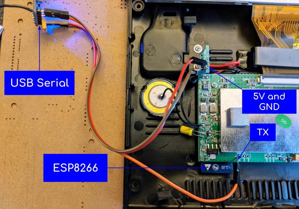
This time I am dealing with a even more sophisticated PWS which combines several different sensors, so the RF signals contain a lot more values that will be very difficult to reverse engineer. I was definitely not looking forward to repeat the same tedious experiments I’ve done a few years ago. However, technology has changed rapidly the past few years. What’s interesting now is that this particular PWS has a receiver unit that is WiFi-capable, and it can even send data to Weather Underground. I was reading its user manual and came across this part: open a browser and type in IP address 192.168.4.1. That immediately caught my attention as that’s the default IP address in AP mode for ESP8266. Ah ha, I bet it has an ESP8266 inside. So I took it apart and there you go, a ESP-WROOM-2 chip laid right in front of my eyes.
Next to the ESP chip are three pins clearly marked TXD, RXD, GND. I wasn’t actually hopeful that the TX pin will send any useful data, but I decided to hook up a USB serial adapter to check it anyways. I soldered three wires to connect the receiver’s 5V, GND, and TXD pins to the serial adapter’s 5V, GND and RX pins.
Hooking up a USB serial adapter
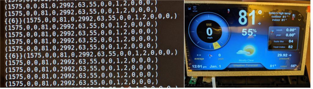
I took a few guesses about baud rate, and found that 115200 is the correct one. Well, I didn’t think it was going to be that easy, but right there on the serial monitor screen, the chip is sending out sensor values in plain text, presumably for debugging purpose. Can’t be easier than this 🙂
Serial output from the receiver unit
You can see that it occasionally print out {{6}}, which probably indicates the current status. Then it’s a sequence of numbers separated by commas. Some of the values are easily recognizable if you look at the LCD screen. For example, 2992 must be the barometric sensor value, 81 and 55 are the temperature and humidity values respectively. But the other values are more obscure, like what is that 1575 value?
Then I remembered this PWS can connect to Weather Underground. Maybe the serial print out will change once it’s set to send data to Wunderground? So I followed the user manual to configure the WiFi settings and typed in a random WU station name (aaa) and a fake key (bbb). You can actually go to Wunderground.com and apply for a proper PWS station name and key, I didn’t do that because I was merely experimenting with the unit so I didn’t want my unit to contaminate the Wunderground data in my area. In any case, once it’s configured, the serial output started showing the HTTP GET command that it’s using to send data to Wunderground. Below is an example:
So now the numbers all make sense: that 1575 value is the wind direction (157.5 degrees), and all values have clear meanings marked by their variable names. At this point, I can easily write a script that parses the serial output and use the data for my own project.
Summary: this PWS turns out to be the easiest wireless sensor I’ve worked with, as it involves practically no reverse engineering effort. I am glad to see that ESP8266 has made into so many WiFi products on the market today. To be fair, this is a lucky example as it prints out all the useful data through serial, so no painful RF decoding effort is necessary. I am not sure so other weather stations would be as easy.
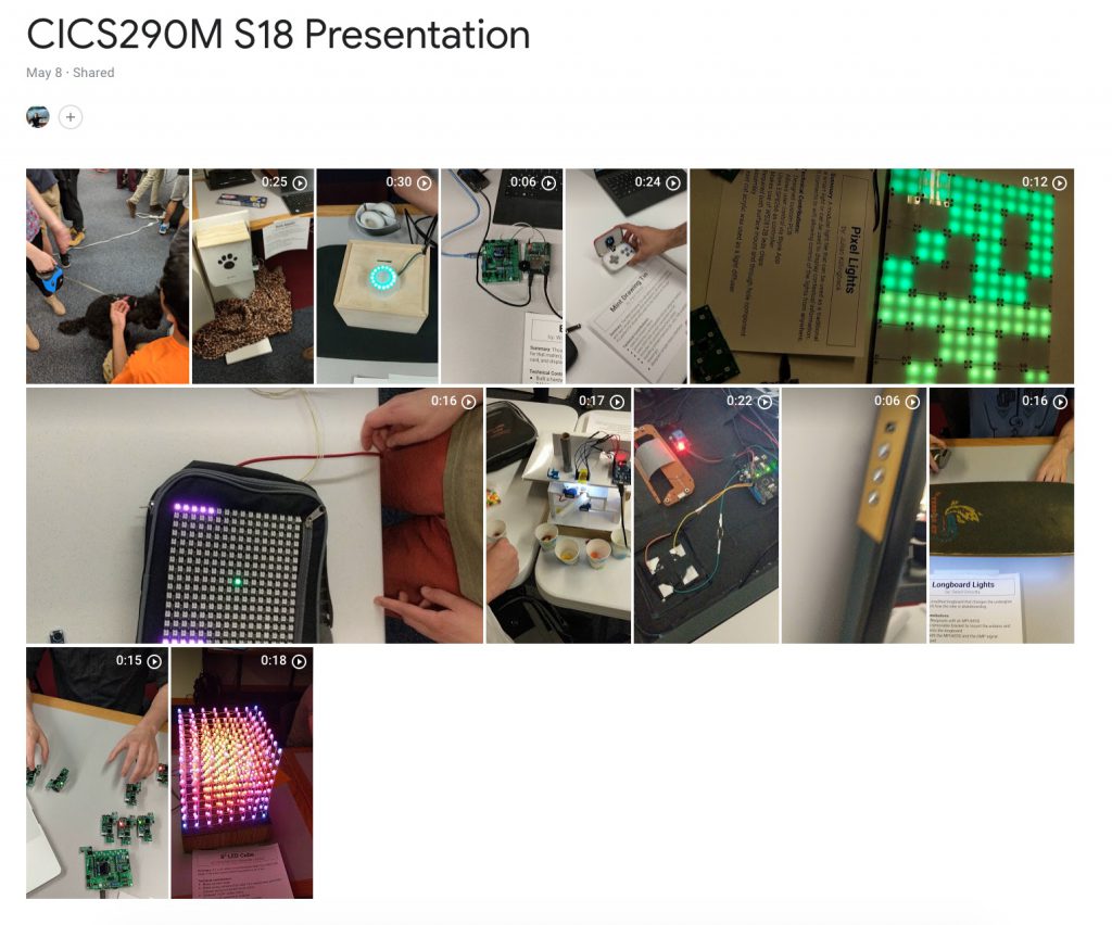
Can’t believe I have been silent on this blog for more than a year now. I would really like to get back to blogging more regularly, and hopefully this post serves as a good starting point. As the first order of business, I would like to showcase a number of student projects from a new class I taught at UMass in the Spring 2018 semester. It’s a brand-new class called Make — A Hands-on Introduction to Physical Computing. It covers basic electronics, circuits, Arduino programming, sensors, actuators, ESP8266, Processing, and rapid prototyping techniques. It’s a rather exciting adventure for me, as it’s the first time this course has ever been offered in my college, and it fulfills the college’s lab science credit. I have both the freedom to choose whatever topics I am passionate about teaching the students, and the burden of designing the complete set of lectures, weekly lab, homework, and exam.
The class ended with a final project where students work in two-person teams for 6 weeks to complete a project of their choice. The basic requirement is that it must be a physical computing project that involves both constructing hardware and developing software. The outcome was really satisfying as many of the projects are truly impressive and/or innovative. It’s particularly so as for many students this was the first time they have ever learned about electronics and Arduino. Below I briefly describe some of my favorite projects. I took videos of some projects, which you can find in this shared Google Photos album. The complete list of 27 project can be found in this folder of Google sites (I asked every team to create a Google site to document their project).
The most ambitious and visually marvelous project is the 8x8x8 Neopixel Cube project by Alex and Chris (warning, the site is loaded with pictures and videos so loads rather slowly). Though there is an abundance of LED cube projects you can find online, this one is based on Neopixels, so it’s a full-color LED cube and it’s slightly easier to solder than standard color LEDs. They’ve done a fantastic job constructing the cube, and solved a number engineering challenges such as power stability issues, and data transfer speed issues by splitting the cube into sections and providing data entry point for each section separately using the FastLED library. I have a video clip showing the project in action. I wish I had taken a longer video because there were a few really cool animations (e.g. visualizing 3D surfaces, video streaming, 3D snake game) that show off just how amazing a Neopixel cube is.
Then there is a smart mirror project, ironically called Dumb Mirror, by Sam. It’s constructed using a two-way mirror, with a Raspberry Pi driving a scavenged LCD display and a Neopixel ring. A Python program grabs time, news, and weather information and displays them to the LCD screen. There are also some buttons on the side for user interaction. I’ve two short video clips (video1 and video2) showing the project in action. It’s aesthetically beautiful and quite functional as well, makes me want to own one myself.
Next in line is the Mint Drawing Tin project by Paul. This is a really cute project constructed using an Arduino nano, 128×64 OLED display, buttons, Lithium battery, and a 3D printed front panel, snugly fit inside a Altoids tin. It’s like a mini version of Etch a Sketch, but much cooler as it can store image frames and play them back as an animation. I have a thing for mint-tin project, as my own journey of Making began many years ago with a mint-tin sprinkler controller.
Some students made custom PCBs for their projects. One of them is the PixelLight project by Julian. It’s constructed by many Neopixel tiles daisy-chained to make a larger display. Each tile is a custom PCB of 10cmx10cm in size containing 4 Neopixels. The original goal was that the user can connect the tiles in an arbitrary manner and the system can automatically identify the topology of the connections. That proved to be a bit of a challenge so in the end he settled with a pre-determined topology. Still, it’s a quite elegant and visually pleasing project, and the display patterns can be changed in dynamically in real-time by using a ESP8266-based microcontroller and the Blynk app.
Another custom PCB project is the Radio Fireflies by Nick and Emily. It simulates how fireflies in nature synchronize their flashing patterns. Each node is a custom-made circuit consisting of an ATtiny85 mcu, color LED, 433MHz RF transmitter and receiver, and buzzer. RF is used to simulate how individual fireflies communicate with each other, eventually leading to synchronized flashing pattern. It’s a cool and ambitious project, though the real-time demo didn’t work very well as the presentation room was full of RF interferences.
A really fun and entertaining project is the Voice-Controlled Pong by Mike and Garret. It’s made of an Arduino, a 16×16 Neopixel matrix, and two microphone sensors. Each of the two players uses their voice to control the movement of the bat, i.e. the louder the sound the higher the bat moves. At first, it looks somewhat silly that the two players just keep yelling ‘Ahhhh’ repeatedly towards the microphone sensors, but when you try it out yourself, you will find it’s absolutely a joyful and entertaining game to play.
And of course there has to be a pet-centered project. The Bone Appétit is a lovely project by Mary and Nick, perfect for pet owners — it’s made of a Raspberry Pi, camera, servo, load cell (for measuring food weight), tucked inside a lovely wooden box. Using a Blynk app, they can monitor the pet, release food up to a pre-defined weight, and snap a picture. The best part of their demonstration is that they brought an actual puppy, who must have had a great time drawing so much attention from the audience.
There are a number of other amazing projects, like color candy sorter, pocket synthesizer, smart curtain, mail checker, pellet stove monitor, secret knock door lock etc. It’s truly delightful and rewarding to see such a range of creative student projects. I am teaching the Make course a second time this semester and will update the post when this semester’s final presentation ends.